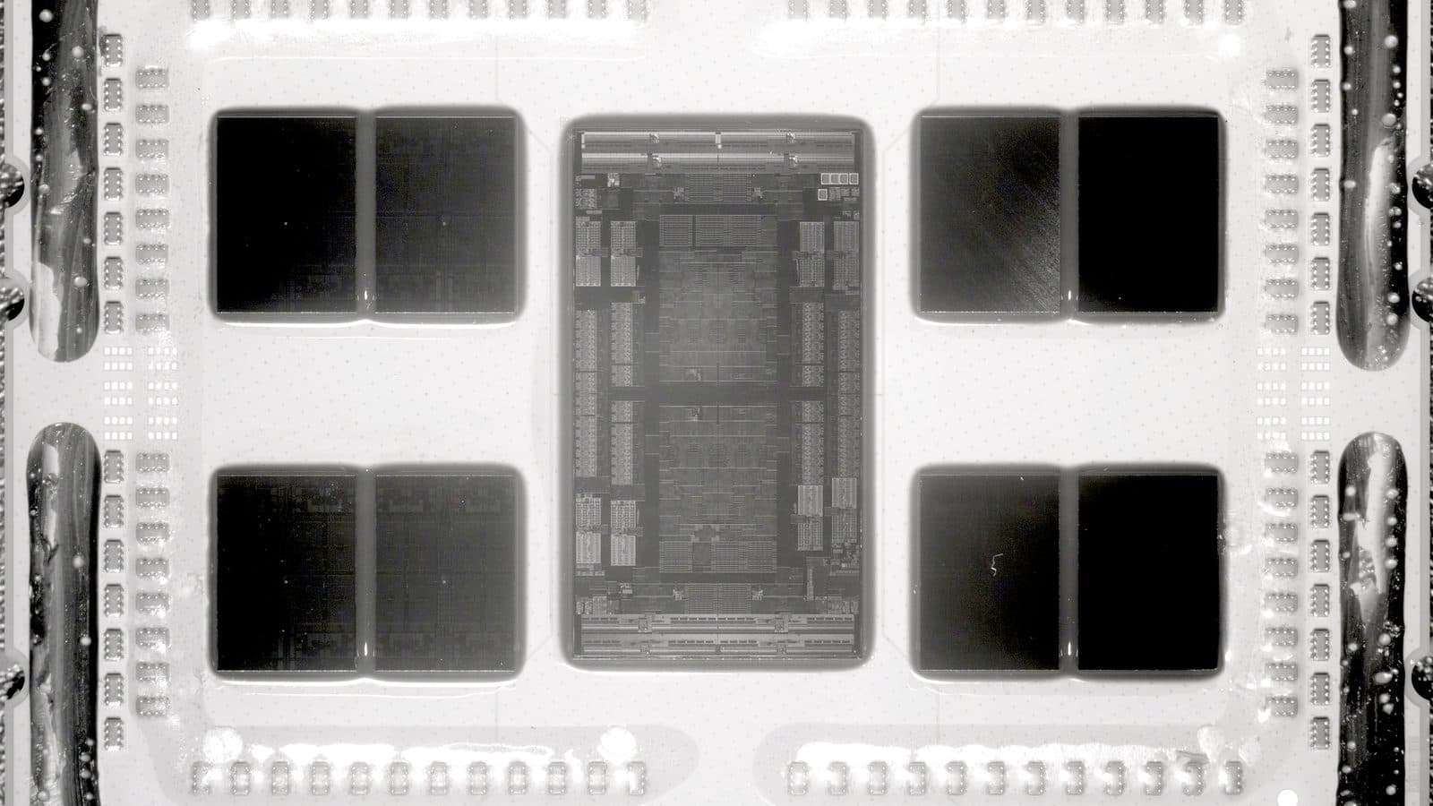


Samsung Opens a Yokohama Packaging Lab to Close Its HBM Gap
Samsung has opened an advanced semiconductor packaging research hub in Yokohama, betting that Japanese materials and toolmakers hold the key to its AI memory ambitions.
By TPW Editorial7 min read