
Advanced Packaging: The New Battleground of the Semiconductor Industry
Smaller transistors no longer deliver big enough gains. How advanced packaging, chiplets, 2.5D/3D stacking, HBM, became the chip industry's battleground.

On this page
For half a century, the semiconductor industry ran on a single bargain: make the transistor smaller, and everything gets faster, denser, and cheaper. That bargain has broken down. The physical work of shrinking transistors continues, but the economic reward has narrowed to the point where the biggest performance gains increasingly come from somewhere else entirely, from how chips are assembled, not how their transistors are drawn.
Related reading: Samsung Opens a Yokohama Packaging Lab to Close Its HBM Gap · Micron's Revenue Nearly Quintuples to a Record $54.23 Billion on AI Memory Demand.
Advanced packaging, once the unglamorous back end of chipmaking, has become the industry's real battleground. It is where memory bandwidth, system performance, manufacturing yield, and cost per compute are now decided. This is a durable shift, not a passing one, and understanding it means understanding why the old lever stopped working.
Why scaling alone stopped being enough
Moore's Law was never only a technology prediction. It was an economic engine. Because transistor density roughly doubled every couple of years while wafer-processing cost per unit area stayed roughly flat, the cost of manufacturing a transistor fell steadily, historically by an average of 20 to 30 percent a year. That decline is what made computing cheap enough to put into everything.
The engine has stalled. Work by Zvi Or-Bach at MonolithIC 3D, later corroborated by Milind Shah at Google, indicated that per-transistor cost stopped falling at the 28 nm node and has been flat to slightly rising since. At the leading edge, analyses of advanced-node economics now describe something closer to an inversion: 2 nm wafers have been reported at roughly $30,000, about 50 percent more than 3 nm wafers, against leading-edge fab costs of $15–20 billion or more.
Three constraints reinforce each other:
- The reticle limit. Lithography tools can expose only so large an area in one pass. In practice that caps a monolithic die at roughly 800 mm², a hard ceiling on how much compute can sit on one piece of silicon.
- Yield economics. Large dies are exponentially more likely to catch a killer defect, so a bigger die means a smaller fraction of good parts per wafer.
- The wrong-node problem. Not every function needs the most expensive transistor. Analog, RF, I/O, and SRAM often get little or nothing from the leading edge, yet they are dragged along if they share a die with the logic that does.
“It may prove to be more economical to build large systems out of smaller functions, which are separately packaged and interconnected.” — Gordon Moore, 1965
Moore himself anticipated the answer decades ago. The industry has spent the intervening years turning that observation into a manufacturing discipline.
What advanced packaging actually is
Advanced packaging is the set of techniques for integrating multiple dies (and sometimes other components, such as memory stacks, passive devices, or optical engines) into a single package, connected by much denser wiring than a conventional circuit board could ever provide. The old view treated the package as protective housing. The new view treats it as the system.
The family spans a spectrum from "2D" (dies side by side on a substrate) through "2.5D" (dies on a shared interposer or bridge layer) to "3D" (dies stacked vertically and connected through silicon), with finer gradations in between that engineers label 2.3D, 3.3D, and 3.5D depending on which layers carry the high-density wiring.
        ┌─────────────────────────────────────────────┐
        │              System board (PCB)              │
        └─────────────────────────────────────────────┘
                   │  package-to-board solder balls
        ┌─────────────────────────────────────────────┐
        │              Package substrate               │
        │      (organic / glass-core / RDL-based)      │
        └─────────────────────────────────────────────┘
             │  C4 bumps · microbumps · hybrid bond
        ┌────────────┬───────────────┬────────────────┐
        │  HBM stack │  Compute die  │   I/O chiplet  │
        │ (DRAM × N) │    (logic)    │                │
        └────────────┴───────────────┴────────────────┘
              └──── interposer / bridges (2.5D) ────┘
The higher you go in that stack, the shorter the wires, the lower the energy per bit, and the harder the manufacturing. Almost every tradeoff in advanced packaging is a version of that.
The toolkit
Interposers and bridges: the 2.5D workhorse
The dominant architecture for high-performance compute places logic dies and memory side by side on a shared silicon interposer, a piece of silicon whose only job is to route dense connections between them. TSMC's CoWoS (Chip-on-Wafer-on-Substrate) is the canonical example. Its silicon-interposer variant supports areas up to 3.3× the reticle (roughly 2,700 mm²); newer RDL-based and bridge-based variants trade some density for cost, flexibility, and the ability to scale even larger. Rather than routing everything through one giant interposer, some designs embed small "bridge" chips or local silicon interconnects only where bandwidth is needed, a cost-conscious middle path.
HBM: memory as a stacking problem
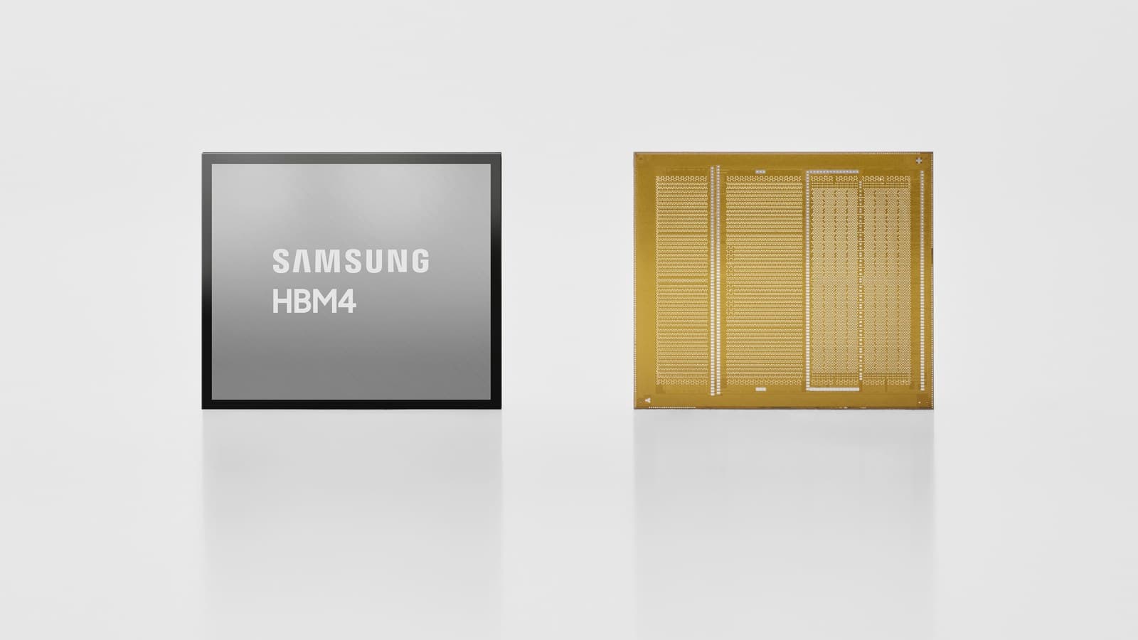
High-Bandwidth Memory is itself an advanced-packaging product: a stack of DRAM dies connected by through-silicon vias, sitting next to a logic die. AI accelerators live or die on how fast they can feed their compute units, which has turned HBM into one of the most strategically important components in the industry.
Stacking HBM higher runs into physics and economics. Current HBM parts stack 8–12 dies; pushing toward 20 or more means the tiny solder microbumps between layers consume too much height and add thermal resistance, as IEEE Spectrum has documented. The migration pathway is toward hybrid bonding and thinner dies, alongside wider interfaces, HBM generations have widened from roughly 1,024 connections to about 2,048, according to industry hybrid-bonding presentations.
Hybrid bonding: going vertical for real
Hybrid bonding joins two dies with direct copper-to-copper connections, no solder. That lets the pitch between connections shrink dramatically: densities of 10,000 to a million connections per square millimeter, at energy below 0.05 picojoules per bit, versus fewer than a thousand per mm² for solder microbumps. The payoff is shorter paths, lower power, and the ability to place cache or memory directly on top of logic. The costs are severe process control, surface preparation, particle sensitivity, and alignment accuracy, which is why dies that pass test are typically bonded die-to-wafer rather than wafer-to-wafer.
UCIe: making chiplets plug-and-play
For chiplet architectures to deliver on their promise of reuse, a die from one vendor has to talk to a die from another. UCIe is the open standard trying to make that happen, defining a die-to-die physical layer, link layer, and protocol stack that maps onto PCI Express and Compute Express Link. The specification deliberately spans two packaging classes (a low-cost standard package for 2D integration and advanced packages for power-efficient 2.5D and 3D) so a single interface design can be reused across products. Later revisions add test, debug, and manageability for multi-chiplet systems as well as higher link rates.
Panel-level packaging: chasing scale
Advanced packaging is currently built mostly on round 300 mm wafers, but the cost of large-area fan-out pushes the industry toward square panels, which waste less material and process more area per step. Yole Group expects panel-level packaging to grow at more than 40 percent a year through 2031, driven by fan-out and 2.5D integration for AI and HPC. Panel-level processes are a leading candidate for keeping large interposers affordable as they grow.
The players and a new division of labor
Advanced packaging redraws the semiconductor supply chain because it sits between front-end wafer fabrication and classical assembly.
- Foundries. TSMC, Intel, and Samsung have made packaging part of their platform offers, bundling it with leading-edge logic so customers get a validated compute-plus-memory-plus-interconnect module. This is a significant source of leverage: leading-edge logic and the packaging that makes it usable increasingly come as one package.
- OSATs and equipment makers. Outsourced assembly-and-test houses and the companies that supply their tools (thermal-compression bonders, hybrid-bonding systems, metrology, and panel-handling equipment) own much of the practical know-how. Equipment demand is shifting toward larger compound dies, chip-on-panel tools, and hybrid bonding.
- EDA and IP. Multi-die design is now a co-design problem spanning the die, the interposer, the package, and the board. It demands a shared data model and new verification and thermal analysis tools, and standard interfaces such as UCIe are what let IP blocks be reused as chiplets rather than redesigned.
The boundary between "foundry," "OSAT," and "systems company" is blurring. Whoever controls the high-density interconnect controls the integration point, and the margin.
The economics: known-good die, yield, and cost per transistor
The reason packaging became strategic is arithmetic.
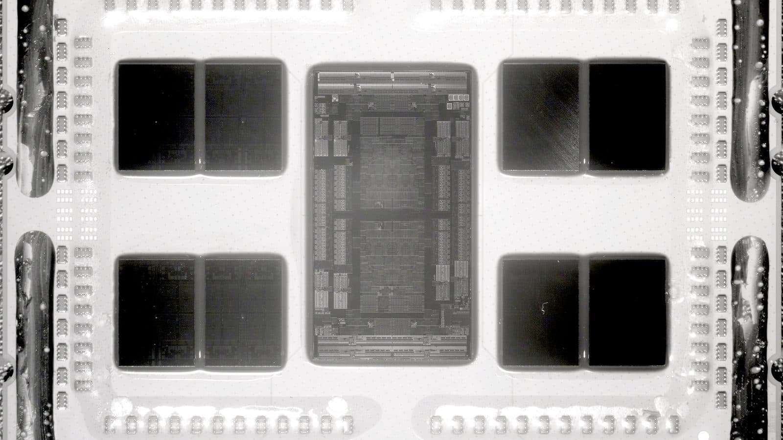
A monolithic die is only as good as its weakest spot. Split it into four smaller dies and a single killer defect ruins only a quarter as much silicon; each die can be tested before assembly and the survivors reassembled. AMD's engineers modeled exactly this for an early chiplet CPU and estimated that the four-chiplet design cost roughly 0.59 times the hypothetical monolithic version, even though it used somewhat more total silicon.
That is the upside. The downside is that packaging introduces its own yield and cost layers:
- Known-good-die testing. Every chiplet must be tested before it is committed to an expensive package. That test adds cost and cycle time, but it prevents a single dead die from destroying a high-value assembly.
- Package-level yield. Bonding defects, interposer defects, warpage, and particles can kill a fully assembled module. Die-to-wafer hybrid bonding helps by letting verified dies bond onto verified base dies.
- Cost of integration. AMD's own white paper lists packaging complexity, lower overall system yield, and latency as real penalties of disaggregation. Splitting a design is not free.
- Substrate availability. Large, warpage-resistant organic and glass substrates are a finite resource, and demand for them has become a bottleneck in its own right.
The net result is that the "cost per transistor" (the metric that once justified every node) is now only part of the story. What matters is cost per package, cost per watt, and cost per unit of delivered performance, and those depend heavily on how well the dies are integrated.
What it means for CPUs, GPUs, and accelerators
The chiplet playbook is now visible across the industry, but it is not applied the same way everywhere.
For CPUs, disaggregation is largely about cost and modularity. A server processor can pair many identical compute dies with a separate I/O die built on an older, cheaper process, then scale the core count and cache simply by adding dies. AMD's modern EPYC generations carry up to 16 compute chiplets around a single I/O die, sharing silicon between product families and harvesting good dies far more efficiently than a monolithic design would.
For AI accelerators, packaging is closer to the product itself. Nvidia and AMD illustrate two different philosophies: one analyst breakdown contrasts Nvidia's B200 (208 billion transistors across two chiplets) with AMD's MI350 at 185 billion transistors across eight, framing it as performance-first versus cost-first. Both approaches concede the same point: the biggest accelerators cannot be built as single dies anymore, so the package (not the transistor) sets the limits on memory bandwidth, power delivery, and scale.
This is also why packaging capacity has become a strategic chokepoint. A design can be ready and the logic wafers can be available, yet the product still cannot ship without interposer, HBM, and assembly capacity. In that sense, the industry's center of gravity has shifted from the fab to the package.
Caveats and open problems
Advanced packaging is not a cure-all, and it introduces new failure modes even as it solves old ones.
- Heat. Stacked dies trap heat, and memory-on-logic and logic-on-logic stacks make cooling harder precisely where power density is highest. Thermal management, not only electrical design, now gates performance.
- Mechanical stress. Materials with different thermal expansion coefficients are bonded together at scale, creating warpage and reliability challenges that grow with package size.
- Power delivery. Large packages with high transient currents stress the power-delivery network; sustaining voltage under rapid load changes is a packaging problem as much as a circuit one.
- Test and debug. Once dies are bonded, they are difficult to probe. Test access, telemetry, and debugging across multiple chiplets are active areas of standardization.
- Ecosystem maturity. Standard interfaces and interoperable chiplets are improving, but the plug-and-play chiplet marketplace is still more aspiration than reality. Many high-volume designs use proprietary die-to-die links.
- Disaggregation's own tax. Splitting work across dies costs latency and performance per watt. For latency-sensitive or cost-sensitive products, monolithic designs can still win.
What to watch
The direction of travel is clear: more dies, denser connections, larger packages, and more of the system's value captured at the integration layer. The interesting questions are about which techniques cross from premium to mainstream.
- Glass substrates and glass interposers, which promise flatter, more dimensionally stable large packages and could ease the warpage problem that limits organic substrates.
- Panel-level packaging, which must prove its yield and uniformity before it can displace wafer-level flows for high-volume products.
- Hybrid bonding in memory, which determines whether HBM can keep stacking higher without breaking thermal and height budgets.
- UCIe and the chiplet ecosystem, where the test, manageability, and compliance features matter as much as raw bandwidth.
- Co-packaged optics, which moves high-speed links from copper traces into the package and could reshape data-center interconnect.
- Advanced-packaging capacity and cost, the practical limit on how fast any of this scales.
None of this makes transistor scaling irrelevant. Leading-edge logic is still where the fastest, most efficient compute lives, and the nodes keep advancing. But the returns now come from combining the right dies in the right package, not from shrinking one die indefinitely. The industry's decisive contests (for performance, for cost, for who controls the stack) are being fought at the package level. That is the new battleground, and it will be for a long time.
The one-sentence version
Transistors still matter, but the gains now come from integration: chiplets, dense die-to-die interconnect, and stacked memory packaged into a single system, which is why packaging, not only lithography, decides what chips can do and what they cost.
Tags

TPW Editorial
Editorial Team
TechPastWeek's editorial team reports and edits every story we publish. We research each piece against primary and credible secondary sources, and a human editor reviews and signs off before it goes live.