
Samsung Opens a Yokohama Packaging Lab to Close Its HBM Gap
Samsung has opened an advanced semiconductor packaging research hub in Yokohama, betting that Japanese materials and toolmakers hold the key to its AI memory ambitions.


On this page
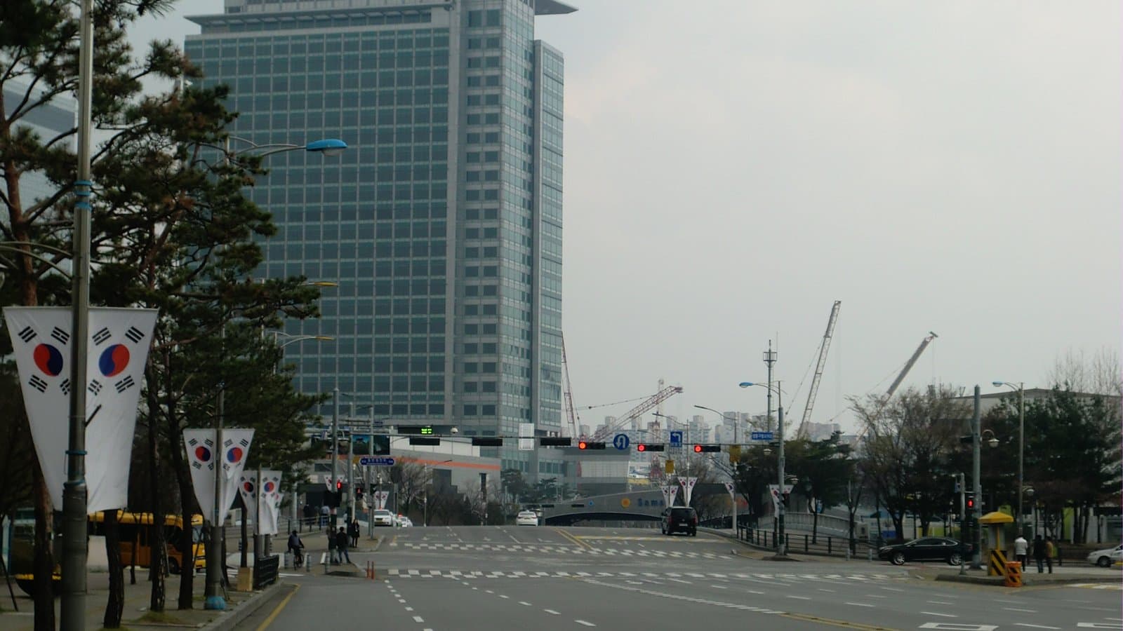
Samsung Electronics opened a semiconductor packaging research centre in Yokohama on September 8, gathering executives, Japanese government officials and supplier representatives at a ceremony in the Minato Mirai waterfront district. The Advanced Package Lab, as the company calls it, is aimed at the back half of chipmaking: the assembly steps that turn bare dies into finished processors, and that have quietly become one of the tightest bottlenecks in the artificial intelligence supply chain.
Related reading: Advanced Packaging: The New Battleground of the Semiconductor Industry · Samsung's Profit Topped 100 Trillion Won for the First Time on AI Memory.
The facility gives Samsung a research base inside the world's strongest cluster of packaging materials and equipment suppliers. Its bet is that proximity to those suppliers will shorten development cycles at a moment when packaging, rather than transistor scaling alone, determines how well an AI accelerator performs.
The opening is small in capital terms and large in strategy. Samsung is investing about 40 billion yen, roughly $260 million, over five years from 2024, and Japan's Ministry of Economy, Trade and Industry is contributing 22.5 billion yen, or about $200 million, of that according to Business Korea. The lab occupies around 6,600 square metres and includes a cleanroom built to run equipment in conditions matching an actual production line.
Why packaging became the bottleneck
For most of the semiconductor era, progress came from shrinking transistors. That approach has run into physical and economic limits at the leading edge, and the industry has shifted attention to how chips are assembled and connected. Modern AI hardware is a system in a package: a graphics processor or other accelerator sits alongside stacks of high-bandwidth memory, wired together by an interposer or a silicon bridge on a shared substrate. How cheaply and reliably those pieces can be joined now shapes both performance and supply.
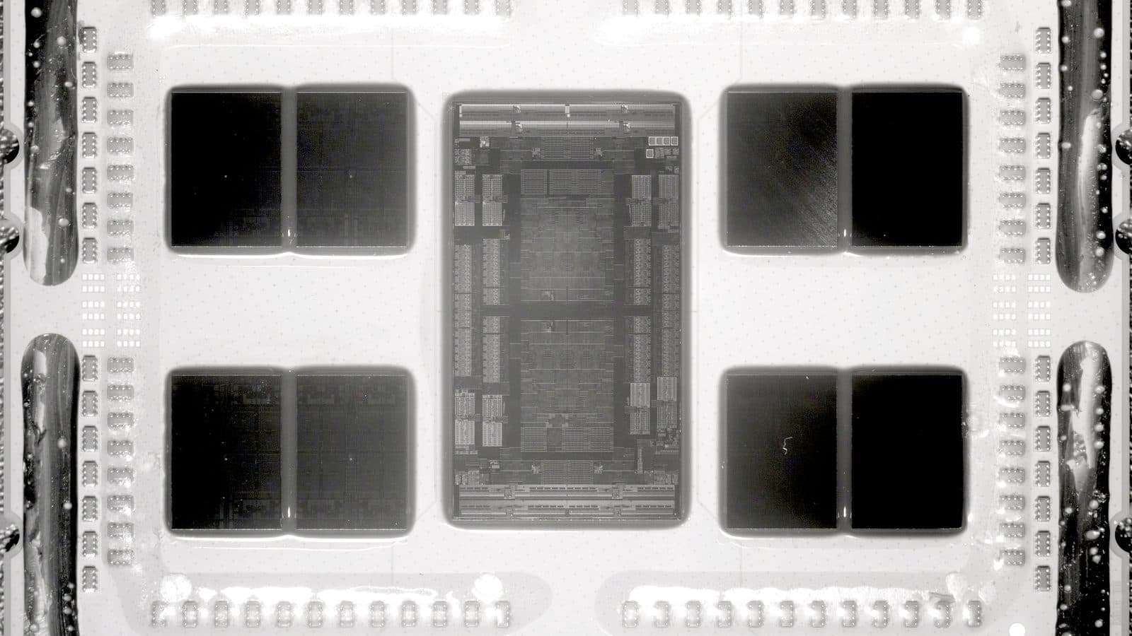
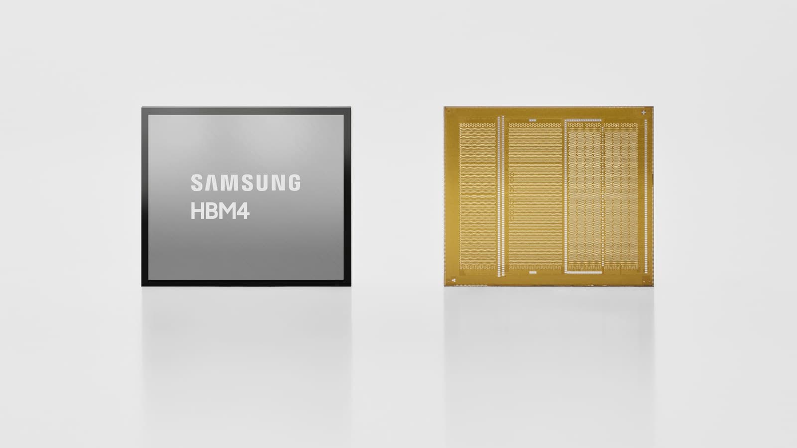
High-bandwidth memory is the clearest example. HBM is built by stacking memory dies vertically and linking them with thousands of through-silicon vias, then bonding the stack next to a logic die. Each generation adds layers and complexity. That work is materials-intensive, and the materials, adhesives and substrates it depends on are largely Japanese. Sumitomo Bakelite holds around 40 percent of the global market for the encapsulants that protect chips from heat, moisture and impact, while Resonac and Mitsubishi Gas Chemical lead in the substrate materials used to stack HBM, according to the Nikkei report relayed by Business Korea.
A Samsung official told the same outlet that assembly technology is complex and “becoming a new bottleneck,” which is why a company that dominates memory overall would build a research hub abroad for this step alone.
Front end, back end
Chipmaking divides into two halves. The front end draws circuits onto silicon wafers at a fab. The back end, sometimes called assembly and test, cuts the wafers into dies and packages them into the finished components that go into systems. Advanced packaging belongs to the back end, and it is where makers of AI accelerators increasingly compete.
The economics explain why the back end has moved to the centre of the industry's attention. A leading-edge wafer can cost tens of thousands of dollars, and it only becomes a sellable product after it is diced, tested and assembled. When the assembly step fails, the money lost is not the packaging cost alone but the value of the dies underneath it, which is why a few points of packaging yield are worth more than they appear. The same dynamic has made third-party assembly and test companies, known as OSATs, strategically important, and it has pushed chip designers to treat packaging as something to co-design with the silicon rather than leave to a subcontractor.
The Japan advantage, and the paperwork it removes
Japan's role in the story is not sentimental. The country supplies a large share of the materials that advanced packaging consumes, and it hosts the equipment makers, universities and research institutes that develop them. Samsung said it works with more than 50 Japanese companies across AI semiconductor back-end processes, and the September ceremony drew 15 partner firms including Tokyo Electron and Ibiden.
The new lab also removes a practical delay. Under the old arrangement, a new material developed by a Japanese supplier had to be shipped to Korea for evaluation, a process that could take up to two months because of chemical substance licensing and import-export procedures. With the Yokohama cleanroom in place, Samsung can evaluate materials and build prototypes locally, then move only the most promising candidates to mass-production lines in Korea. The company framed the change as an acceleration of the loop between development and production.
Talent is the other motive. The greater Tokyo area concentrates specialists in semiconductor materials and equipment, and Samsung said it plans to grow the site's research staff past 100 by 2027. It started with 95 Korean and Japanese researchers, a mix intended to move knowledge in both directions rather than treat Japan purely as a supplier.
The race Samsung is trying to win
The strategic backdrop is Samsung's position in HBM. The company is the largest memory maker by revenue, but in HBM it has trailed SK Hynix, its Korean rival, through the first generations of the technology that AI accelerators rely on. Nikkei framed the Yokohama investment as an attempt to catch up by strengthening ties with Japanese suppliers, calling AI semiconductors a contest of cross-border industrial alliances rather than single companies.
That framing fits the wider market. Nvidia's accelerators depend on HBM stacks made by a small group of suppliers, and packaging capacity has been the final step that gates finished output. TSMC's chip-on-wafer-on-substrate lines, which package accelerators with HBM, have been oversubscribed for two years. Any memory maker that can improve yield and throughput on the packaging side has a direct route to winning more of that business, because the constraint that limits accelerator shipments is as much assembly as it is wafer supply.
There is also a policy layer. Japan has spent heavily to rebuild its semiconductor base, and its support for the Samsung lab is part of a broader effort to make the country a node in the AI supply chain rather than a supplier of parts to it. Cooperation between Korean and Japanese firms has warmed after years of friction over export controls and historical disputes, and governments on both sides now treat the semiconductor industry as strategically linked.
One lab among many
Samsung's Yokohama site joins a crowded set of packaging investments. TSMC is expanding its advanced packaging lines in Taiwan and building others abroad, Intel has made packaging central to its foundry pitch, and memory rivals are adding capacity of their own. The competition is less about who invents the first bonding method than about who can ramp it at high yield and low cost.
Caveats and what to watch
The claims attached to the opening are Samsung's own. The lab has been operating in stages since it was established in 2023, and the ceremony marks its full-scale operation rather than a product milestone, so there is no yield or performance figure yet to judge. The company is not saying which packaging technologies the Yokohama team will prioritise, or how its work will connect to specific HBM generations. The spending, at roughly $260 million, is modest next to a memory fab, and a research hub does not by itself close a manufacturing gap.
The relevant measures to watch sit elsewhere. The first is HBM share and qualification: whether Samsung wins places in the accelerator programmes that determine volumes, and whether it narrows SK Hynix's lead in the newest HBM generation. The second is yield, the number that decides whether packaging capacity translates into shippable product. The third is whether the Japan collaboration produces faster cycles in practice, moving from materials evaluation to production in months rather than the old two-month evaluation round trips alone. The fourth is geopolitical: if the Korea-Japan semiconductor partnership deepens, it changes how supply chains for AI hardware are drawn, and which countries sit inside them. The fifth is cost. Advanced packaging is more labour and materials intensive than front-end wafer work, and it carries wider margins for the companies that master it, so a yield advantage on the back end converts into pricing power as well as volume.
For now, the clearest reading of the Yokohama opening is that Samsung sees packaging as a competitive variable it cannot afford to outsource, and that it believes the shortest path to improving it runs through the Japanese suppliers who make the materials it needs. The lab is a wager that being near those suppliers is worth more than owning the process alone.
Cover image: “Minato Mirai - Yokohama Skyline March 2025” by Justin Taylor via Wikimedia Commons, CC BY 2.0.
Tags

TPW Editorial
Editorial Team
TechPastWeek's editorial team reports and edits every story we publish. We research each piece against primary and credible secondary sources, and a human editor reviews and signs off before it goes live.