
TSMC to Lift 2nm and 3nm Output as AI Demand Outruns Supply
TSMC is raising advanced-node capacity sharply, targeting a roughly 70% increase in 3nm wafer output over 18 months as AI chip demand outstrips supply.

On this page
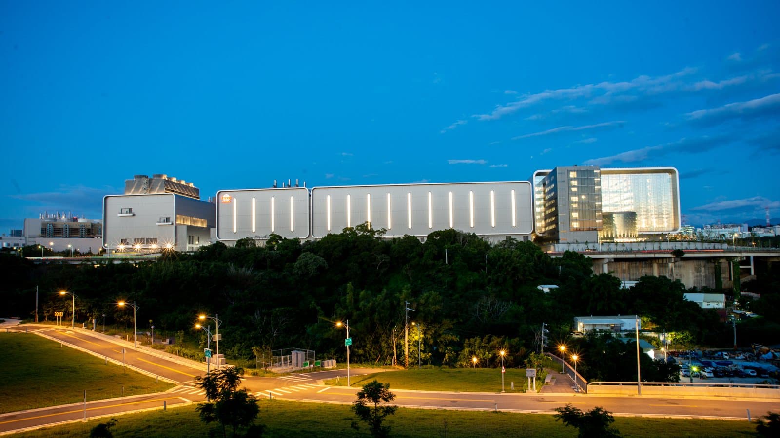
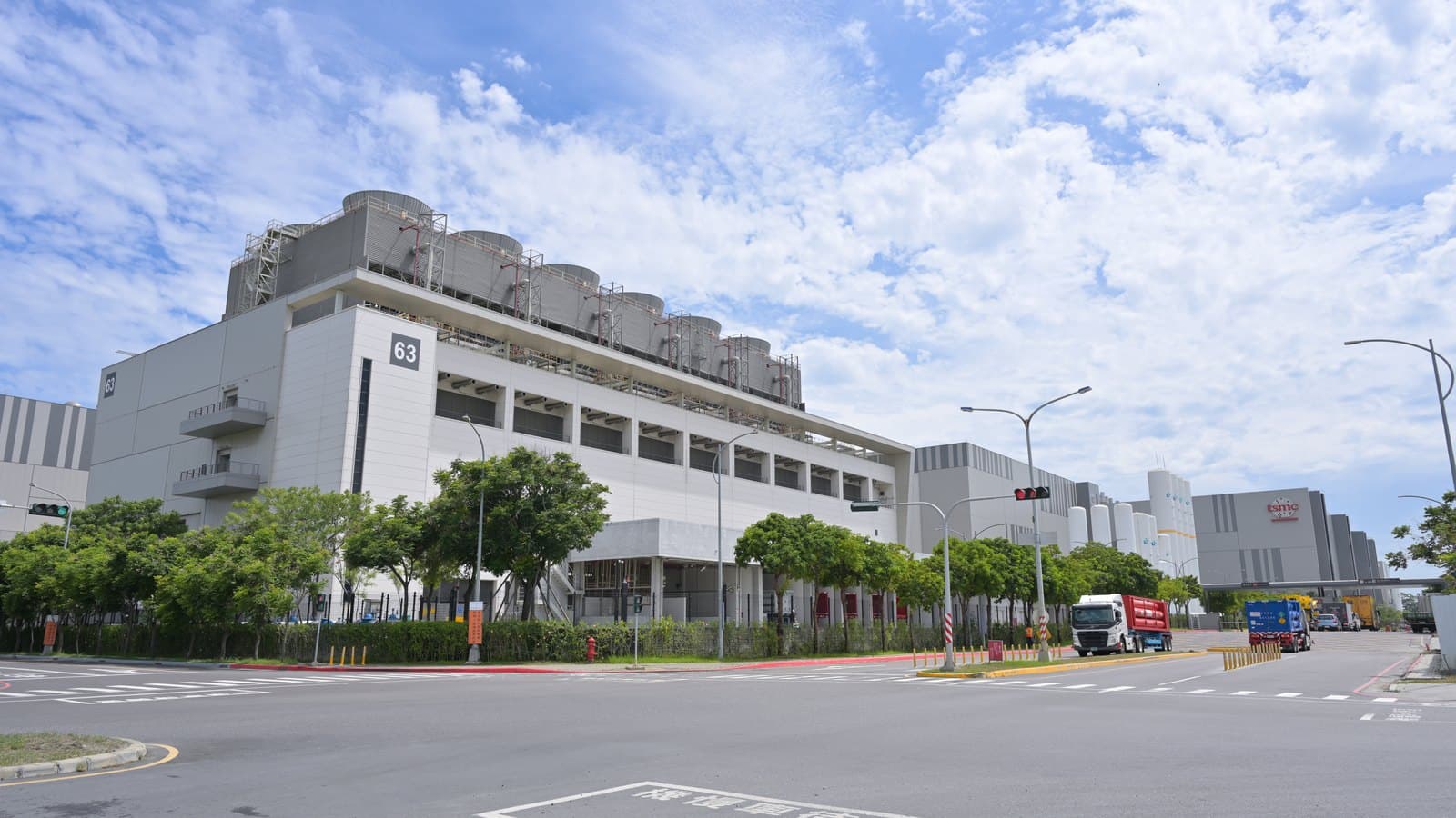
Taiwan Semiconductor Manufacturing Company has begun a broad expansion of its leading-edge manufacturing capacity, telling customers it will increase output of its 2-nanometer and 3-nanometer processes through next year as demand for AI accelerators keeps running ahead of supply, according to supply-chain reports published in Taiwan on 14 September.
Related reading: TSMC Posts a Sixth Straight Record Quarter as AI Demand Outruns Supply · Taiwan Plans to Make Unauthorised AI-Chip Exports to China a Crime.
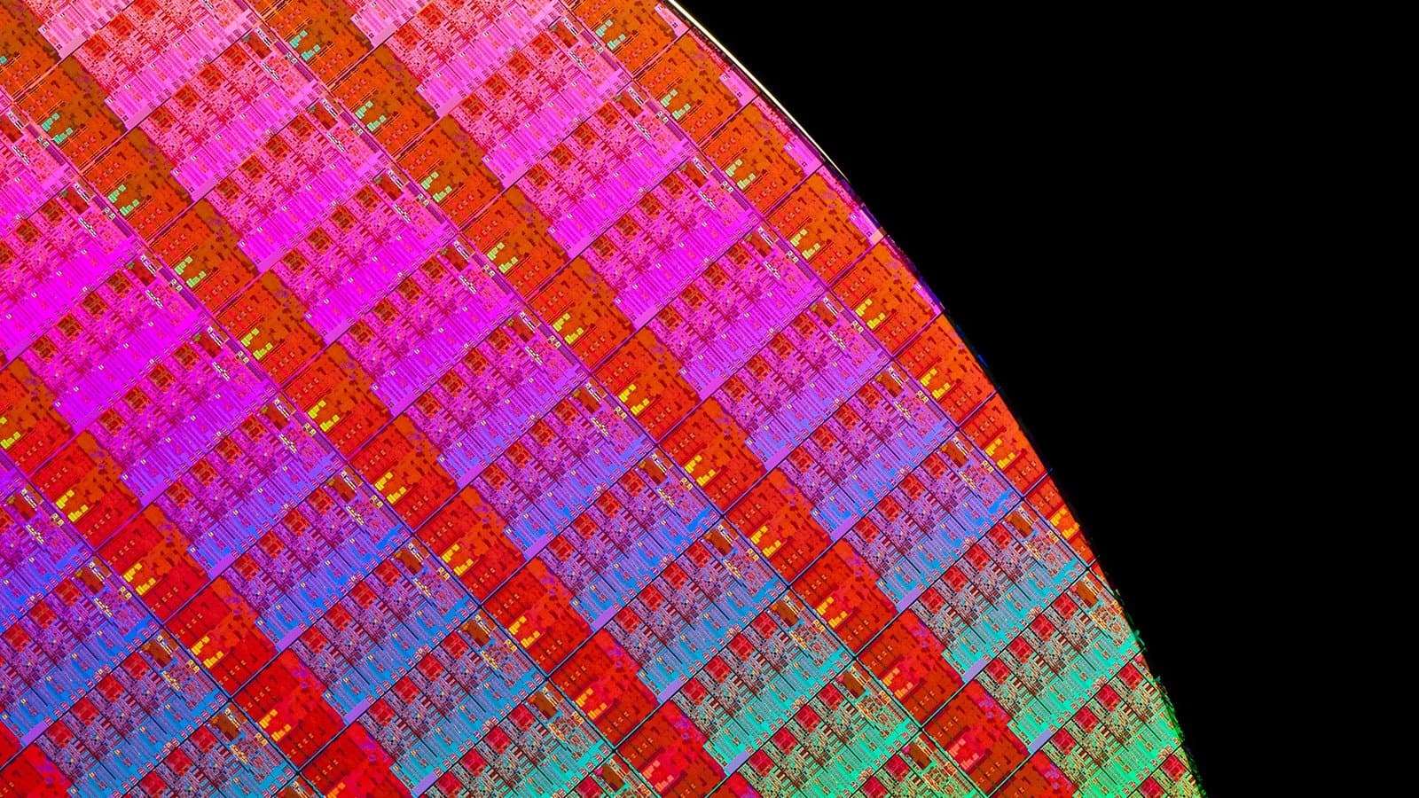
The figures reported by United Daily News and other Taiwanese outlets, and summarized by BigGo and the Seoul Economic Daily, describe a foundry running close to its physical limits. Monthly 3-nanometer wafer output is expected to climb from between 120,000 and 130,000 at the end of 2025 to about 180,000 by the end of this year, then to roughly 210,000 a month by the middle of 2027. That is an increase of about 70 percent across 18 months. The newer 2-nanometer node is smaller in absolute terms but is ramping at a similar pace: output is projected to reach 90,000 wafers a month by the end of 2026 and about 110,000 by mid-2027, a gain of roughly 22 percent.
TSMC declined to confirm the internal targets, and the company does not publish customer-level capacity plans. The direction, though, is consistent with what executives told investors in July, when the company raised its full-year capital-spending guidance to between $60 billion and $64 billion, up from about $50 billion, and said 70 to 80 percent of that would go to advanced processes.
The demand side has not slowed
The expansion is a direct response to AI infrastructure spending. Nvidia's data-center GPUs, the accelerators that anchor most large training and inference clusters, are built on TSMC's advanced nodes, and the company's next-generation Rubin platform is expected to drive the largest share of the 3-nanometer ramp. AMD, Broadcom and the hyperscalers building custom silicon all rely on the same leading-edge capacity.
Analysts cited by Taiwan's Economic Daily News and TrendForce expect 3-nanometer revenue to overtake 5-nanometer for the first time in the second half of 2026, with quarterly output value for the node exceeding NT$400 billion, or more than 30 percent of total revenue. That milestone matters because it shows where the money in the foundry business now sits. The smartphone cycle that once defined each node transition has been replaced by a multi-year AI build-out whose buyers sign commitments years in advance.
TSMC said on its July earnings call that it had secured order visibility through 2029 and 2030, an unusually long horizon for a business that historically measured backlog in quarters. "Demand for AI chips built on advanced processes was very strong," the company told investors, adding that contracts with major customers and cloud service providers continued to grow.
Three countries, one bottleneck
To add that capacity, TSMC is pursuing a build-out spread across three geographies. It is constructing additional 3-nanometer wafer fabs in Taiwan, in Arizona in the United States and in Japan, while converting some existing 5-nanometer lines to 3-nanometer production. The conversion work is the fastest lever because it reuses already-depreciated equipment, but it also carries risk: if AI demand were to soften, TSMC would be left with less capacity for the mature nodes that still serve broad markets.
Advanced packaging is expanding alongside the front-end lines. TSMC is adding capacity at its AP7 plant in Chiayi and building packaging capability in Arizona to meet demand for chip-on-wafer-on-substrate, the process that integrates GPU dies with high-bandwidth memory. The company aims to reach roughly 260,000 CoWoS wafers a month by the end of 2028. Packaging, not transistor density, has been the tightest constraint on AI accelerator shipments for the past two years, and it remains the piece that determines how many finished chips reach customers.
Samsung and Intel are chasing the same demand from lower positions. Samsung's Taylor, Texas fab has reportedly improved its 2-nanometer yield to around 80 percent, a level that would make the site commercially competitive if it holds, and the company is deepening talks with Qualcomm while serving as a second source for Broadcom-designed parts. Intel has built a lead in high-NA extreme ultraviolet lithography, having run its millionth high-NA test wafer, and is pitching its 18A process to sovereign and hyperscale customers. OpenAI's confirmation that Samsung Foundry has joined its custom-silicon program as a production and research partner shows how quickly the second-source option has moved from theory to commercial discussion.
None of that yet threatens TSMC's position. The company makes an estimated 95 percent of the world's most advanced AI chips, and every major custom accelerator announced so far, from Google's TPU to Amazon's Trainium to OpenAI's Jalapeño, was designed around a TSMC process.
What the ramp costs, and who pays
A capacity plan of this size is expensive in ways a wafer-count table does not capture. TSMC raised its capital budget to between $60 billion and $64 billion for the year, and the depreciation that follows a build-out of that scale lands on the income statement for years, regardless of whether every tool is fully used. Leading-edge wafer prices are already the highest in the industry, and customers have in recent years accepted prepayments and take-or-pay terms to secure allocation. Those terms shift risk toward the buyers, which is tolerable while AI demand compounds and painful if it plateaus.
The expansion also depends on suppliers that are themselves at capacity. Each new leading-edge fab needs extreme ultraviolet lithography tools from ASML, deposition and etch equipment from Applied Materials, Lam Research and Tokyo Electron, and a workforce able to install and qualify all of it. Equipment lead times are long, and the same suppliers serve Samsung and Intel, which are building at the same time. A fab shell can be finished on schedule and still sit empty if a tool is late.
Memory and packaging compound the constraint. AI accelerators pair logic dies with high-bandwidth memory, and HBM production is concentrated among a small number of suppliers whose capacity is booked well ahead. TSMC's CoWoS packaging lines are the final step before a finished accelerator ships, and they have been the tightest link in the chain for two years. When packaging is the bottleneck, adding wafer capacity at the front end does not translate one-to-one into finished chips.
There is a geopolitical layer as well. Concentrating the most advanced manufacturing in Taiwan is a strategic vulnerability that the United States and Japan have spent years trying to dilute, and TSMC's Arizona and Japan fabs are partly a response to that pressure. Those sites cost more to build and operate than the Taiwan equivalents, which means the capacity being added outside Taiwan is likely to carry a higher cost per wafer. Customers who want a non-Taiwan source are, in effect, paying for redundancy that also serves a policy goal.
The roadmap beyond 2nm
TSMC is not waiting for the current nodes to mature before preparing the next ones. The company has said its A16 process, its first angstrom-class node at 1.6 nanometers, is on track, and is developing A14, A13 and A12 technologies. To support those nodes, it is working with ASML on 12-inch photomasks, a change that would let more dies be printed per exposure.
The roadmap raises a question that hangs over the whole industry: whether the physics and the economics of each successive node can keep pace with the ambitions of the AI labs buying them. A16 and its successors are expected to bring backside power delivery and other structural changes, but they also cost more per wafer and are harder to yield. The customers lining up for them are betting that performance per watt, not headline density, is what determines whether a data center earns its cost of capital.
What to watch
Three signals matter for the rest of this year. The first is whether TSMC's 2-nanometer ramp reaches its stated targets without a yield stumble, which would validate the decision to wait longer than Samsung and Intel before adopting gate-all-around transistors. The second is capex discipline: a $60-billion-plus budget has to be justified by demand that arrives on schedule, and a single delayed hyperscaler program can leave a fab line under-used. The third is whether the second-source projects, in Texas and Arizona, convert from memorandums into wafer starts. If they do, the pricing conversations at the leading edge change; if they stall, TSMC's grip on the AI supply chain tightens further.
For now, the company's message to the market is straightforward. It can add capacity faster than it can add customers, and the customers are still lining up.
Tags

TPW Editorial
Editorial Team
TechPastWeek's editorial team reports and edits every story we publish. We research each piece against primary and credible secondary sources, and a human editor reviews and signs off before it goes live.