Google Adds a Confidential TPU and a Dual-Chip 8i Max, Its Fourth System This Year
Google announced TPU 8tx for confidential inference and TPU 8i Max with two chips per package on 9 November. Neither has a price or a shipping date yet.

On this page
Key takeaways
- Google Cloud announced TPU 8tx, for confidential inference, and TPU 8i Max, a two-chip package for long contexts, on Monday 9 November 2026.
- Both are system configurations around existing eighth-generation TPU silicon; Google says 2026 is the first year it has introduced four TPU systems.
- TPU 8tx uses the same silicon as TPU 8t with 5th Generation AMD EPYC host processors, and Google claims up to 2x lower latency than 8t with a near-zero performance penalty.
- TPU 8i Max doubles the compute, SRAM and HBM bandwidth of TPU 8i by putting two 8i chips on one package in the existing rack footprint.
- Google published no price, no availability date and no absolute specifications; Bloomberg reported, citing Amin Vahdat, that both systems will be available in 2027.
Google Cloud added two systems to its eighth-generation TPU line on Monday 9 November: TPU 8tx, built for confidential inference, and TPU 8i Max, which pairs two TPU 8i chips on a single package for long-context work. Both are system configurations built around silicon Google already sells. Neither is a new chip. The company says 2026 is the first year it has introduced four TPU systems, after TPU 8t and TPU 8i at Google Cloud Next in April.
Related reading: Advanced Packaging: The New Battleground of the Semiconductor Industry · Nvidia's DSX POD Turns an AI Factory Into a Shipping Container.
The two systems answer different buyer questions. One is whether a regulated customer can run a model on data it is unwilling to expose. The other is whether an agent workload that runs out of memory bandwidth can get more of it inside the same rack. Google's post gives no price and no availability date for either.
Amin Vahdat, Google's chief technologist and senior vice president for AI and infrastructure, wrote the post. Bloomberg reported that both systems are expected to become available in 2027, and that Vahdat told the outlet they would be available that year (Quartz). Google's own text does not commit to a date.
Four systems, two dies
The eighth-generation family now has four members, and they rest on two pieces of silicon. TPU 8t handles scale-up training, with Google claiming up to 2.7 times better training performance than the previous generation. TPU 8i handles low-latency reasoning, with an 80% improvement in inference price-performance, again by Google's measure. TPU 8tx takes the 8t silicon and adds hardware protection for data in use. TPU 8i Max puts two 8i chips in one package.
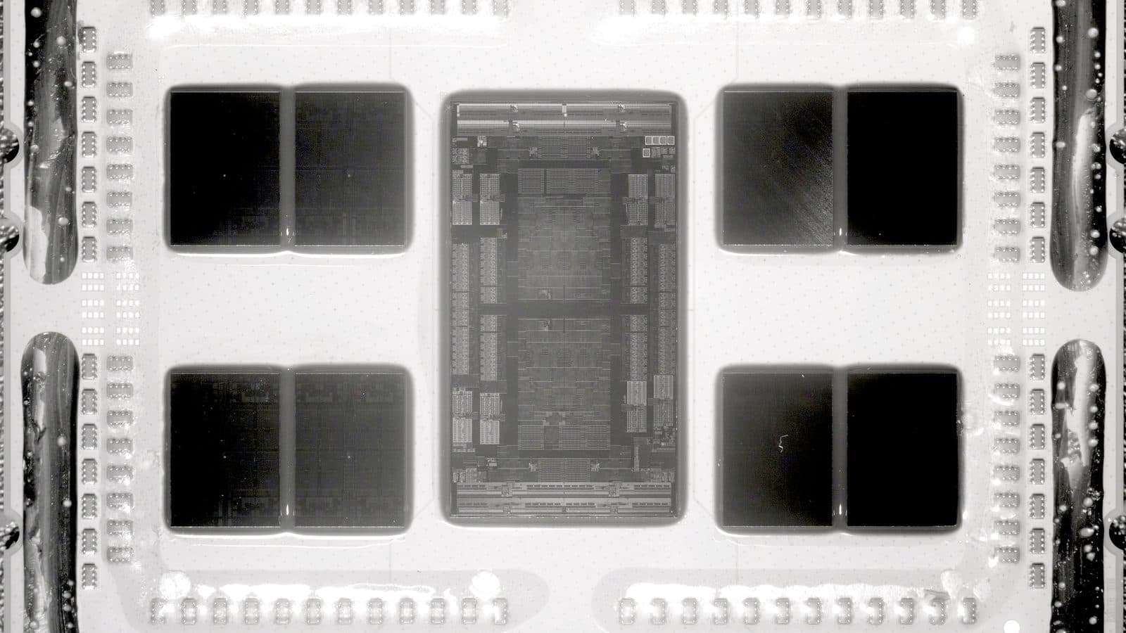
A system configuration is everything in a machine that is not the die: the package, the board, the host processors, the network fabric and the security firmware. Changing those can shift what a data center can do without a new process node, and Google says it can now do it in months rather than years.
Two dies covering four systems is a cheaper cadence than four design cycles. The risk sits in what a launch post cannot show, namely whether the software treats the variants as one platform.
The 8tx sells confidentiality as a product
TPU 8tx is the third system in the generation and the one with the clearest commercial trigger. It uses the same silicon as TPU 8t, paired with 5th Generation AMD EPYC host processors, and adds hardware-level isolation for sensitive data and model weights while they are in active use. Ordinary cloud encryption stops at the memory boundary: data is decrypted while a processor works on it, and that window is what confidential computing closes.
Google is aiming the system at regulated enterprises and governments running frontier or proprietary models and autonomous agents alongside sensitive data. The workloads it names are fine-tuning on private data, distilling a large model into a smaller one, and training agents through reinforcement learning. The pitch is that all three can happen on one system without moving sensitive data between clusters.
The 8tx also uses the low-latency Boardfly network Google built for real-time reasoning, and the company claims up to 2x lower latency than TPU 8t with a near-zero performance penalty. Protection in use usually costs something in throughput or response time; Google is saying the bill here is close to nothing.
No independent security audit or certification was announced. The isolation is described by Google and has not been tested in public by a third party, which is the kind of evidence regulated buyers usually ask for before putting sensitive data on a shared cloud. For those buyers the 8tx stays a candidate.
The 8i Max doubles the package
TPU 8i Max is the fourth system. It combines two low-latency TPU 8i chips on one package, which Google says doubles compute, SRAM and HBM bandwidth against a single 8i. Because it uses the existing rack footprint, the company frames the gain as more computing power per square foot and per watt. The workload it targets is an agent working across an entire codebase or hours of video at once, where memory bandwidth is the constraint.
Every token a model generates reads a cache that grows with the context window, so a long session spends its time moving memory rather than doing arithmetic. Two chips on one package double the bandwidth available to that cache, provided the software can address both dies as one device. Google has not published the details that would settle whether it can.
Google also published no absolute specifications, which has not stopped others from producing some. MarkTechPost took the published per-chip TPU 8i figures, 10.1 PFLOPS in FP4, 288 GB of HBM, 8,601 GB/s of bandwidth and 384 MB of SRAM, and multiplied them by two. That yields about 20.2 PFLOPS, 17.2 TB/s and 768 MB of SRAM. Those are arithmetic on Google's numbers, not a Google datasheet, and they assume the package scales linearly.
Linear scaling is the assumption worth watching. A dual-chip package shares a substrate, a power envelope and a cooling budget, so the second die does not always deliver a clean doubling at rack level.
Why packaging became the roadmap
The four-system year is a claim about cadence, and cadence is the part of the TPU business Google most wants to contrast with Nvidia. Google's pitch is that packaging, memory, networking and security can be re-cut around the same silicon on a much shorter cycle. That lever is cheaper to pull than a new process node, and it addresses the constraints buyers hit: bandwidth per rack, isolation, and latency.
The competitive set includes Nvidia's Rubin platform, Microsoft's Maia 200 and AWS Trainium3, among others. Nvidia remains the dominant merchant supplier of accelerators, and nothing in Monday's announcement changes that. Google's TPUs are sold through Google Cloud and, increasingly, deployed directly into customers' own data centers, according to the blog.
Google describes TPUs as “a rapidly growing business with nearly 100 customers.” — Amin Vahdat, chief technologist and SVP of AI and infrastructure, Google, 9 November 2026
That customer figure is unaudited and comes without a revenue split, so it measures breadth rather than scale. Google lists frontier labs, trading firms, retailers and universities among the users. It does not say how much of the business is external, how much is Google's own Gemini training, or what any of those customers pay per chip-hour.
Vendors across the accelerator market are adding memory and bandwidth around existing silicon. For the Chinese side of that race, see our report on DeepSeek's Huawei Ascend pretraining plans.
The software stack is where the switching cost moved
Google also announced software changes that matter more to a buyer's total cost than any single specification. TorchTPU was open-sourced last month, so PyTorch code and Hugging Face models run natively on TPUs, with TPU backends for vLLM and SGLang. A new open-source TPU agent suite, in preview, plugs into Claude Code, Cursor and Google Antigravity to automate onboarding, diagnose bottlenecks and autotune kernels in plain language.
There is also a new open-source XLA Serving Engine, which lets teams train in Python and serve in a low-latency C++ runtime across TPUs, GPUs and CPUs. Agent Compute Engine suspends and resumes idle agent sessions to cut infrastructure spend. TPU Sync, an open-source model-state layer, tiers KV caches across HBM, host DRAM, shared storage and the data-center network, and Google says it cuts KV transfer latency and time to first token by more than 90%. Cloud Pathways, the distributed runtime behind Gemini, is now generally available on GKE, and GKE dynamic slicing is generally available with Google claiming up to 5x faster job startup and up to 4.5x faster fault recovery.
Google cites state-of-the-art price-performance on the InferenceX and AgentX benchmarks using its native vLLM-TorchTPU stack, with new evaluations from SemiAnalysis. Those are Google's chosen benchmarks, run on Google's own software stack. They are evidence that the stack is no longer the weak link, not a like-for-like comparison with a competitor's rack on a workload neither company picked.
The switching cost has moved to that stack. A rival can match a chip specification on a datasheet. Matching a compiler, a set of tuned kernels, a serving engine and an orchestration layer takes longer, and that is what Google is building. The gains accrue to teams inside Google's stack; a team running another framework, or its own kernels, gets less of the improvement.
What Google did not say
Google's post is long on architecture and short on what a buyer needs to sign a contract. There is no price, no availability date, no region list, no instance type and no datasheet. Most performance numbers are ratios against earlier Google products, which say how much better the new system should be than the old one and nothing about how it compares with an Nvidia rack.
The missing numbers
The 2x latency, 2x compute, 2x SRAM and 2x bandwidth figures are Google's own, measured against its own earlier parts, and none has been independently verified. The TPU Sync result, a cut of more than 90% in KV transfer latency, was measured on Ironwood, the previous generation, not on 8tx or 8i Max. No third party has published a benchmark or a security audit for either new system.
The 2027 date comes from Bloomberg rather than from Google. Vahdat told the outlet the systems would be available that year, and the company's post does not repeat the commitment (Gizmodo). Buyers planning capacity for next year will have to treat the date as a report.
Confidential computing has a similar gap. Google says the 8tx protects data in use at the hardware layer, and no certification body has confirmed that. The feature is a purchasing requirement in finance, healthcare and the public sector, and those buyers tend to ask for an attestation report rather than an architecture diagram.
A price per chip-hour, and whether 8i Max is sold as a whole rack or a slice of one, would turn a capability claim into a budgeting input. A named customer running 8i Max in production, with the bill before and after, would carry more than a benchmark chart. An independent test against Rubin or Trainium3 on the same model would settle the comparison Google avoids, and a third-party certification would decide whether regulated buyers can use the 8tx at all.
Until one of those lands, the two systems exist as specifications and demonstrations. Google has four TPU systems for 2026 and no shipping date of its own for the two newest.
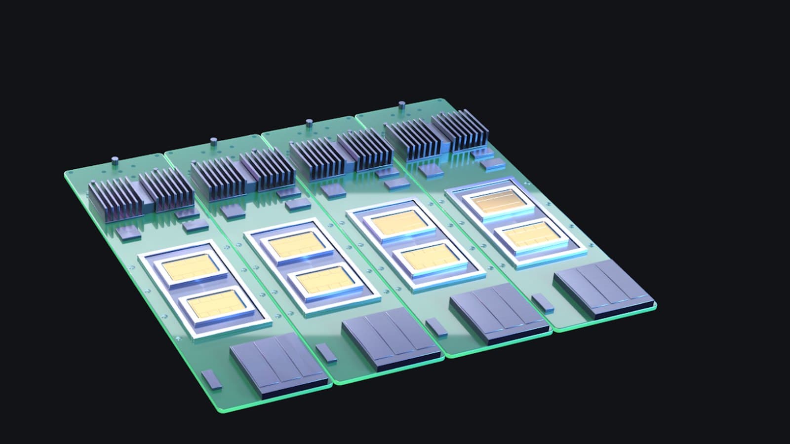
Cover image: Google's official render of the TPU 8tx and TPU 8i Max boards.
Tags
Frequently asked questions
- What is Google TPU 8tx?
- TPU 8tx is a Google Cloud system for secure and confidential inference. It uses the same silicon as TPU 8t, pairs it with 5th Generation AMD EPYC host processors and adds hardware-level protection that keeps data and model weights isolated while they are in use. Google is aiming it at regulated enterprises and governments running proprietary models and agents next to sensitive data.
- What is TPU 8i Max?
- TPU 8i Max is a package containing two low-latency TPU 8i chips. Google says it doubles compute, SRAM and HBM bandwidth compared with a single 8i chip and fits twice the silicon into the same rack footprint, aimed at agents working across an entire codebase or hours of video.
- When will TPU 8tx and TPU 8i Max be available?
- Google's announcement gives no availability date. Bloomberg reported that both systems are expected in 2027, and Amin Vahdat, Google's chief technologist for AI and infrastructure, told the outlet they will be available that year. That is Bloomberg's reporting, not a commitment in Google's blog post.
- Are the performance figures for the new TPUs official?
- The performance ratios Google published are its own claims and have not been independently verified for these systems. The absolute figures circulating for TPU 8i Max, about 20.2 PFLOPS in FP4 and 17.2 TB/s of bandwidth, were calculated by MarkTechPost by doubling the published per-chip TPU 8i numbers, and are not Google specifications.

TPW Editorial
Editorial Team
TechPastWeek's editorial team reports and edits every story we publish. We research each piece against primary and credible secondary sources, and a human editor reviews and signs off before it goes live.