
China's CXMT Reaches 11.95nm DRAM Without ASML's EUV Tools
CXMT said on 20 September 2026 that its fifth-generation DRAM platform is in mass production, using quadruple patterning to reach an 11.95nm array half-pitch without EUV.

On this page
Key takeaways
- ChangXin Memory Technologies said on 20 September 2026 that its fifth-generation DRAM platform, called G5, has entered mass production.
- CXMT says the platform reaches an 11.95nm active-area half-pitch in the memory array using quadruple patterning rather than ASML extreme ultraviolet lithography.
- Two 24-gigabit LPDDR5X products built on G5 entered volume production, in 496-ball and 245-ball packages for smartphones and portable devices.
- CXMT says the process produces at least 50 percent more dies per wafer than its fourth-generation platform, a figure that counts total dies before defect screening.
- Counterpoint Research puts CXMT's share of global DRAM revenue near 10 percent, making it the fourth-largest memory maker behind Samsung, SK Hynix and Micron.
Chinese memory maker ChangXin Memory Technologies said on 20 September 2026 that its fifth-generation DRAM platform, known as G5, has entered mass production, and that two 24-gigabit LPDDR5X products built on it are already shipping. The company announced the milestone at the 2026 World Manufacturing Convention in Hefei, the eastern Chinese city where it is based.
Related reading: SK Hynix Posts a Record 104.6 Trillion Won Quarter as HBM4 Ramps · Samsung's Profit Topped 100 Trillion Won for the First Time on AI Memory.
The claim that matters is not the number of bits. It is the process. CXMT says G5 reaches an active-area half-pitch of 11.95 nanometres in its memory array using self-aligned quadruple patterning, a route that does not require ASML's extreme ultraviolet lithography machines. Chinese chipmakers have been cut off from those tools under US-led export controls since 2023, and the assumption behind the controls was that the ban would hold advanced memory manufacturing back. CXMT's own announcement describes the platform as closing the gap with the most advanced memory technologies in volume production.
What CXMT actually announced
The two new products are 24-gigabit LPDDR5X dies, one in a 496-ball package and one in a 245-ball package, aimed at mid-range and flagship smartphones and other portable devices. At 24 gigabits, a single die holds 3 gigabytes, which CXMT says is 50 percent more data than the comparable previous-generation part.
Alongside the density gain, CXMT reported several process changes. The memory array's capacitor aspect ratio reaches 45:1, supported by a redesigned process flow and new materials. The platform uses a DRAM-optimised high-k metal gate process, which CXMT says cut the core cell array height to 6,762 nanometres. The company also said it built a digital-twin system over its existing process modules to shorten development cycles.
The most consequential number for cost is density. CXMT says the number of dies produced per wafer, converted to an 8-gigabit basis, rose by at least 50 percent compared with its fourth-generation platform. TrendForce reported the same figure, noting that more dies per wafer improves both power efficiency and the cost per chip.
Read the fine print: the 50 percent figure counts total dies before defect screening, which is not the same as yield. CXMT did not disclose its yields or its monthly output for G5.
That distinction is worth holding on to. A memory maker's economics depend on how many of those dies are good, and neither CXMT nor the analysts summarising its announcement published a yield number. The density gain is real and meaningful, but it is an input to the cost calculation rather than the finished result.
The same caution applies to the 11.95 nanometre figure. It measures the half-pitch of the active area, one specific structure inside the memory array. Samsung, SK Hynix and Micron market their processes with rounded, branded labels such as 12-nanometre class, and those names do not map cleanly onto CXMT's measurement. As the Seoul Economic Daily noted, the two types of number are difficult to compare directly.
Why quadruple patterning is the whole story
Extreme ultraviolet lithography prints very fine features in a single pass. Without it, manufacturers reach smaller dimensions by exposing and etching the same layer several times, a technique called multiple patterning. Quadruple patterning, self-aligned or otherwise, does that four times over.
The trade-offs are well understood. Each extra pass adds process steps, time and opportunities for defects, which is why quadruple patterning is more expensive per wafer than a single EUV exposure. The payoff is that it works on the deep ultraviolet tools Chinese fabs can still buy. CXMT's G5 platform is a demonstration that the ceiling imposed by export controls is higher than the controls' designers assumed, even if the route is slower and costlier.
The memory market is the place where this matters most. DRAM is a commodity with thin margins and enormous capital requirements, and it has been dominated for years by three players. CXMT, founded in 2016 with backing from the Hefei city government, barely registered in global rankings four years ago. Counterpoint Research data cited in coverage of the launch puts its share of global DRAM revenue near 10 percent in the second quarter of 2026, up from roughly 4 percent a year earlier, making it the world's fourth-largest memory maker. Samsung alone holds close to 38 percent, with SK Hynix and Micron filling out the rest of the top tier.
The memory price shock G5 does not fix
The launch lands in the middle of a genuine supply crunch. Data-centre operators are buying high-bandwidth memory for AI servers, and manufacturers have shifted capacity toward those higher-margin parts and away from commodity DDR5. The result has been a sharp rise in retail memory prices. Mainstream 32GB DDR5-6000 kits now sell for $400 to $480, and 16GB modules that cost under $10 in September 2025 have been climbing toward $30 a year later.
TrendForce reported that global DRAM industry revenue jumped 59.5 percent quarter on quarter in the second quarter of 2026, with supply expansion lagging demand growth. Micron broke ground on a $9.3 billion fab in July to add capacity, but that plant will not ship a chip until 2028.
CXMT's first G5 products do not relieve that pressure. They are mobile LPDDR5X parts for phones, not the desktop and server DDR5 modules where prices have spiked, and CXMT's overall volumes remain small next to Samsung or SK Hynix. A fourth credible supplier scaling production changes the long-run arithmetic on memory scarcity, but it does not change this quarter's pricing.
Where the new chips go: the two G5-based products are 24-gigabit LPDDR5X dies in 496-ball and 245-ball packages, aimed at smartphones and portable consumer electronics. They are not the DDR5 modules driving the current desktop and server price surge.
The export controls G5 was built around
The backdrop to the announcement is a set of restrictions that the United States, the Netherlands and Japan tightened from 2023 onward. ASML is the only company that builds extreme ultraviolet lithography machines, and those tools are the most direct route to the smallest features on a wafer. Denying them to Chinese manufacturers was intended to slow progress at the leading edge, and much of the debate since has assumed it would.
Quadruple patterning is the workaround that makes the assumption questionable. It is not a new idea: chipmakers used multiple patterning to push deep ultraviolet tools through several generations before EUV arrived, and the technique is well understood. What is new is applying it at this density in high-volume memory production, where cost per bit decides whether a product is competitive. SAQP raises the number of process steps and the risk of defects, so CXMT's claim rests as much on manufacturing discipline as on the patterning trick itself.
The strategic logic runs in both directions. For Beijing, a domestic memory maker that can reach advanced densities without banned equipment reduces exposure to export controls and gives Chinese device makers a local source of supply. For Washington, the announcement complicates a policy that has been justified partly by the idea that cutting off EUV would set a firm ceiling on Chinese capability. A slower, costlier path to the same density is still a path.
What to watch
Two questions will decide how much G5 matters. The first is yield. If CXMT can turn its density advantage into competitive yields at volume, the cost case improves quickly, and the company becomes a more serious fourth supplier. If the quadruple-patterning route proves too defect-prone, the density gain may not translate into margin.
The second is where CXMT points the platform next. LPDDR5X for phones is a large market, but the strategic prize is the memory sold into data centres, where demand and pricing are strongest. TrendForce noted that CXMT recently announced LPDDR6 mass production and a debut in Xiaomi's 18 Fold, which suggests the company is advancing on more than one front.
There is a broader signal here too. For years the export-control debate assumed that blocking EUV access would hold Chinese memory makers at a fixed technical level. CXMT's G5 does not refute that logic so much as complicate it. A slower, more expensive path to advanced memory still counts as a path, and the company has government backing and a domestic market large enough to absorb it.
Rivals will read the announcement as a warning rather than an immediate threat. Samsung, SK Hynix and Micron still control the high end and the most profitable parts of the market, and the DDR5 shortage is a pricing problem that only new capacity will solve. But a credible fourth entrant at 11.95 nanometres changes how the industry plans its next few years of capital spending, and it undercuts a piece of conventional wisdom that Washington had come to rely on.
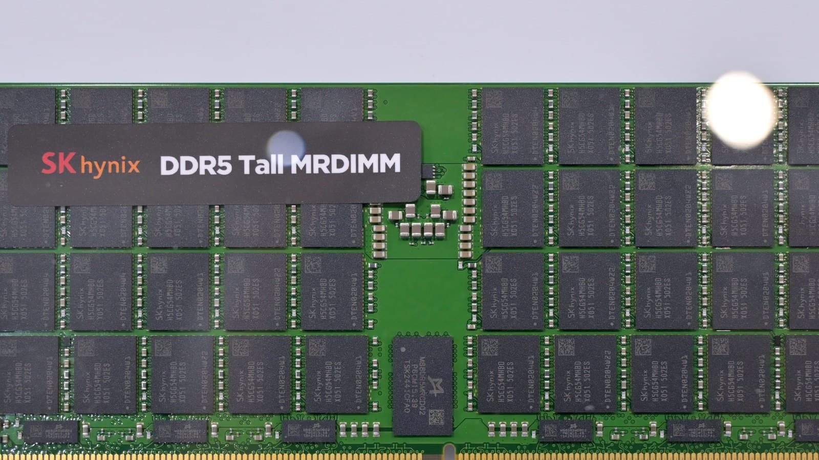
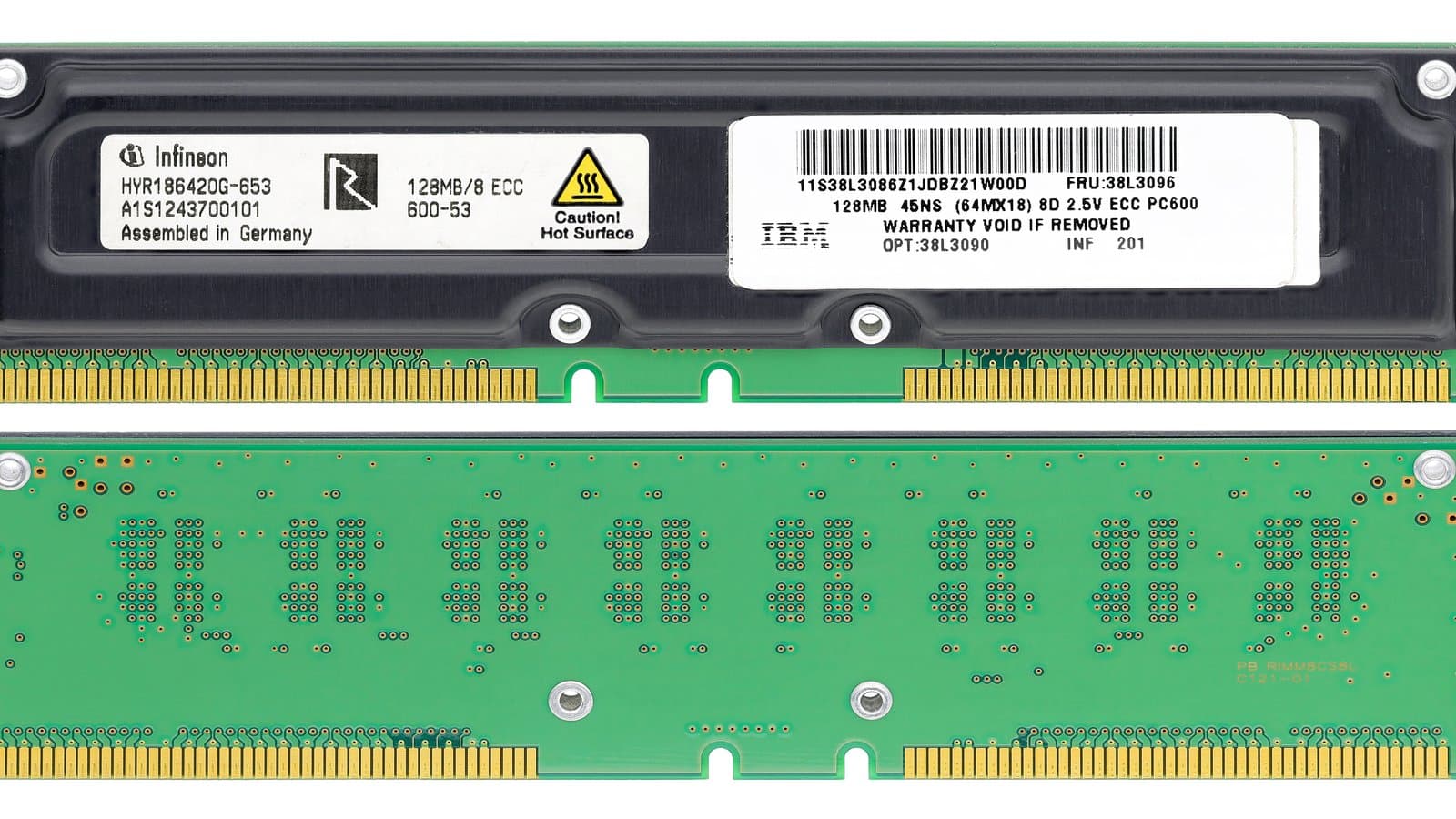
Cover: Wikimedia Commons photo of a DRAM memory module by Mister rf (CC BY-SA 4.0).
Tags
Frequently asked questions
- What is CXMT's G5 DRAM platform?
- G5 is ChangXin Memory Technologies' fifth-generation DRAM manufacturing platform. CXMT announced on 20 September 2026 that it has entered mass production, alongside two LPDDR5X products built on it.
- Does CXMT use ASML EUV machines for G5 DRAM?
- No. CXMT says G5 uses self-aligned quadruple patterning to reach an 11.95nm active-area half-pitch in the memory array, a technique that works with deep ultraviolet tools rather than ASML's extreme ultraviolet machines, which are restricted for Chinese chipmakers under export controls.
- How does 11.95nm compare with Samsung and Micron process names?
- It is not directly comparable. CXMT's figure measures one physical structure, the active-area half-pitch in the memory array, rather than a branded logic-chip process node such as a 12nm-class label.
- Will CXMT's G5 chips lower DDR5 memory prices?
- Not directly in the short term. The first G5 products are mobile LPDDR5X chips for phones, while the DDR5 shortage that pushed desktop and server module prices up is driven by data-centre demand for high-bandwidth memory.

TPW Editorial
Editorial Team
TechPastWeek's editorial team reports and edits every story we publish. We research each piece against primary and credible secondary sources, and a human editor reviews and signs off before it goes live.