
Intel Has Run a Million High-NA Wafers, and Its Rivals Just Adopted Its Standard
Intel says it has processed more than a million High-NA EUV wafers, roughly three-quarters of the world total, as TSMC and Samsung sign on to the mask standard it championed.

On this page
At the SPIE Photomask Technology and EUV Lithography conference in Monterey, California, Intel Foundry and ASML used the same stage to make an unusually specific claim: Intel has now processed more than one million 300-millimetre wafers on ASML's High-NA EUV scanners. By ASML's own accounting, that is roughly three-quarters of every High-NA wafer the entire industry has ever exposed.
Related reading: EUV Lithography, Explained: How the Chip Industry Prints at 13.5 Nanometers · Intel's Data Center Revenue Rose 78% and the Stock Fell 28.58%.
The figure is cumulative and deliberately broad. It includes Intel's research-and-development work, tool-certification runs and volume production, a distinction the joint announcement did not hide. Only some of those wafers are commercial product, selected layers on a subset of Intel Core Ultra Series 3 processors, code-named Panther Lake, built on the company's 18A process. Even so, the milestone moves High-NA EUV from a laboratory curiosity to something closer to a factory workhorse, and it came as Intel's two closest rivals publicly aligned themselves with the direction Intel has been pushing for more than three years.
TechRadar reported the announcement alongside ASML's own numbers from the SEMICON Taiwan conference earlier in September: the company's EXE-series High-NA systems had collectively exposed more than 1.35 million wafers, with ten systems running across four customers and three more being shipped or installed. Intel's share of that total works out to about 74 percent.
A machine that costs as much as a small fab
High-NA EUV is the next step beyond the standard EUV lithography that has defined leading-edge chipmaking for a decade. The "high numerical aperture" refers to a larger opening that gathers more light, which lets a scanner print finer features in a single pass instead of splitting a layer across multiple exposures. That is the promise, and it comes with a price: the machines cost as much as $350 million apiece, and the ecosystem around them (masks, resists, metrology and handling equipment) has to be rebuilt for the larger optics.
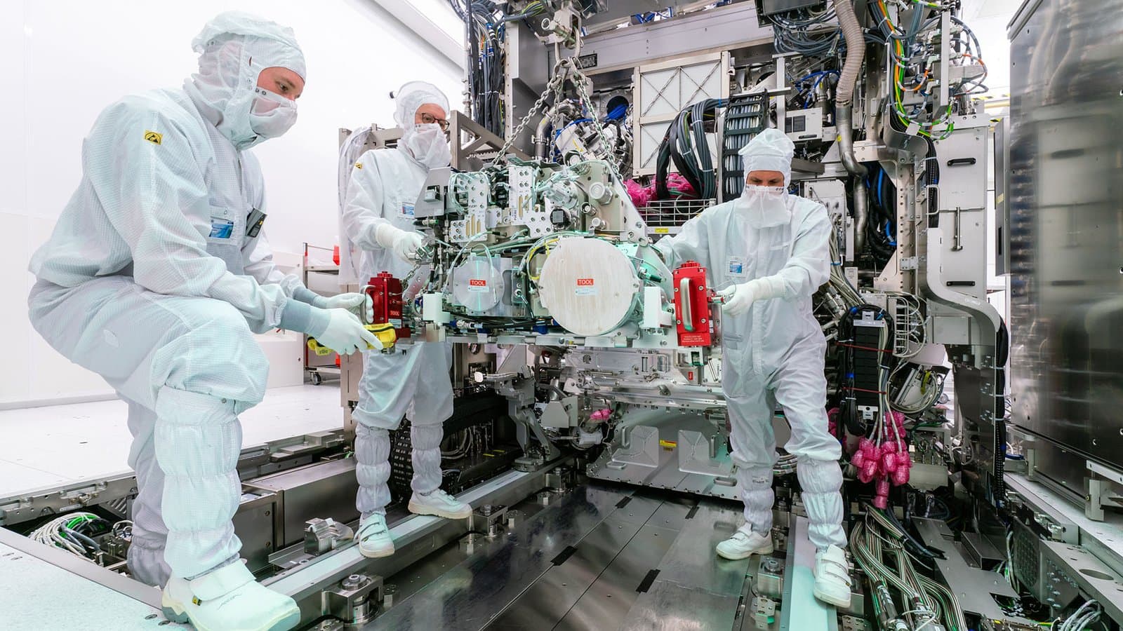
Intel's fleet is small and specialised. The company runs two ASML Twinscan EXE:5000 research systems and at least one EXE:5200B production scanner, which it was the first customer to install and certify in 2025. The EXE:5200B offers throughput of 175 wafers per hour in single-exposure mode and overlay accuracy of 0.7 nanometres, along with better availability than the original tool. Intel's cumulative wafer count, according to TechTimes, has gone from roughly 30,000 wafers in late February 2025 to more than a million in about 19 months.
That ramp is the substance behind a claim Intel has made repeatedly and, until now, somewhat lonely: that it is the only company running High-NA lithography on a shipping product. The joint release with ASML notes that overlay, throughput and availability were meeting Intel Foundry's expectations, and that 18A products using High-NA for selected layers met or exceeded performance achieved with ASML's older NXE platform. For a company that spent much of the past few years being written off in the AI race, the lithography lead is one of the few advantages it can point to that competitors cannot quickly match.
What “a million wafers” does and does not mean
Intel's total deliberately bundles R&D and certification runs with production. It is a measure of experience with the tool, not of chips shipped. Intel does not break out how many Panther Lake wafers used High-NA layers, and neither does ASML, so the number is best read as a technology-maturity figure rather than a manufacturing-volume one.
The mask standard is the real prize
The more consequential news may have arrived a day earlier. On September 7, ASML and TSMC jointly announced an industry initiative to move the photomask format from today's 6-inch standard to a 12-inch (6×12) format built for High-NA EUV. The plan targets a 12-inch mask pilot line by 2031 and full High-NA lithography readiness for advanced-node production by 2033.
For more than three years, Intel had led that campaign largely alone among high-volume logic makers, working with ASML, mask suppliers, EDA vendors and materials companies to build the standards and infrastructure a larger mask format would require. TSMC's formal participation changes the calculus. As The Herald Business put it, the world's dominant contract chipmaker has now publicly committed to the same destination, a signal that the 12-inch format is necessary to fully exploit High-NA for the densest layers in the AI era, a conclusion Intel reached years earlier.
A bigger mask sounds like an incremental detail. It is not. A photomask is the stencil that patterns a layer of circuitry onto a wafer; the size of that stencil determines how much of a chip's layout can be printed at once. The current 6×6-inch standard forces chipmakers to "stitch" together multiple exposures to cover a full field, a workaround that adds complexity and yield risk. Moving to 6×12 would remove much of that stitching, but it requires replacing or substantially modifying mask blanks, deposition and etch tools, inspection and metrology equipment, pellicles, mask writers, cleaning systems and handling robotics across the entire supply chain. ASML's current roadmap for its EXE scanners through 2033 is designed around the existing format, and neither ASML nor Intel has publicly confirmed that shipped tools can be retrofitted.
That is why TSMC's signature matters. Standards only get built if the largest buyers demand them, and TSMC is the largest buyer. The initiative effectively sets a deadline for the whole equipment industry to converge, with 2033 as the earliest date the standard might begin reshaping production economics.
Three roadmaps, one direction
The announcements mapped out how differently the three big makers are approaching the technology. Intel is furthest along and is using High-NA in production today. TSMC laid out concrete plans to apply High-NA to advanced-process mass production starting in 2030, a slight retreat from earlier language that had pointed to 2029, and consistent with its stated belief that multi-patterning with existing 0.33-NA EUV tools can carry its roadmap through its A13 and A12 nodes around 2029. Samsung, meanwhile, said it aims to be the first in the industry to apply High-NA to advanced DRAM mass production, targeting 2028, with the sub-10-nanometre 0a generation the likely candidate; SK hynix told Reuters it is reviewing participation in the 12-inch mask consortium and also targets 2028 for High-NA in DRAM.
The convergence matters beyond bragging rights. High-NA and the larger mask format are, in effect, the next moat around advanced chipmaking, arriving at a moment when China is pouring resources into building its own EUV capability. The non-Chinese camp (ASML, Intel, TSMC and Samsung) is now jointly defining the standards and infrastructure for the generation after current EUV, which puts the frontier several years further out of reach for anyone still trying to master the previous step.
The economics of being early
The value of Intel's head start is easiest to see in what the alternative costs. Standard EUV has carried the industry since the mid-2010s, but pushing it to ever-smaller features requires multi-patterning: printing the same layer in several passes to achieve the resolution a single High-NA exposure can manage. Each additional pass adds process steps, raises the risk of defects, lengthens cycle time and consumes more of the fab's limited capacity. The reason only Intel has committed to High-NA at volume, while TSMC waits until 2030, is that the tools are expensive and the surrounding ecosystem is immature. The reason Intel is willing to pay that price is that it is trying to leapfrog rather than match, a strategy that only works if the technical lead converts into manufacturing yield before competitors arrive.
That conversion is not guaranteed. Getting a scanner to run reliably is a different achievement from getting a process to yield at commercial rates, and Intel's fabrication roadmap has slipped before. The million-wafer figure says Intel has accumulated more operational experience with the tool than anyone else; it does not yet say that experience has produced a cost advantage. The coming quarters (as Panther Lake and later 18A products ramp) will show whether the lead is real in the only place it counts, on Intel Foundry's balance sheet.
The mask-format initiative raises the stakes further. If the industry does move to 12-inch masks by the early 2030s, the transition will be expensive for everyone, and the companies that helped write the standard will be best positioned to absorb it. Intel spent three years arguing for the larger format with little company. TSMC's decision to join does not hand Intel the market, but it does validate the bet, and it means the next generation of lithography will be built around a standard Intel helped define rather than one imposed on it.
The cost of being first
None of this makes Intel's broader position comfortable. Intel Foundry posted $5.76 billion in revenue in the second quarter of 2026, up 31 percent year over year, but still carried a $2.1 billion operating loss, and chief executive Lip-Bu Tan is still trying to win external logic customers at scale. AMD's finance chief, Jean Hu, used a Citigroup conference in early September to say that AMD expects to keep TSMC as "our primary supplier on the wafer side," closing off a foundry opportunity Intel had been hoping to contest. Intel's stock has nonetheless soared more than 150 percent this year, helped by Nvidia's and the US government's decisions to take stakes in the company, a reminder that Intel's strategic value to Washington partly rests on exactly this kind of manufacturing capability.
The High-NA milestone, then, is best understood as evidence rather than a scoreboard. It shows that Intel can run the most advanced lithography tool in the world at meaningful scale, that the tool performs as advertised, and that the industry's dominant players have accepted Intel's argument about the next mask standard. Whether that translates into profitable foundry business is a separate question, and one that depends less on physics than on customers. But for a company whose fab ambitions were widely doubted, being the only one with a million wafers of High-NA experience (and having rivals adopt the standard it championed) is about as strong a technical case as Intel could have made this quarter.
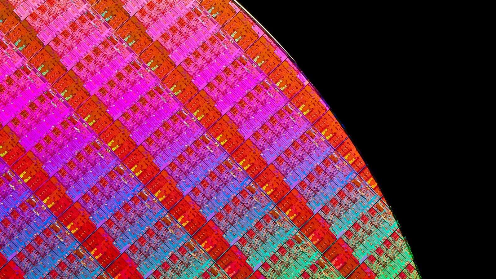
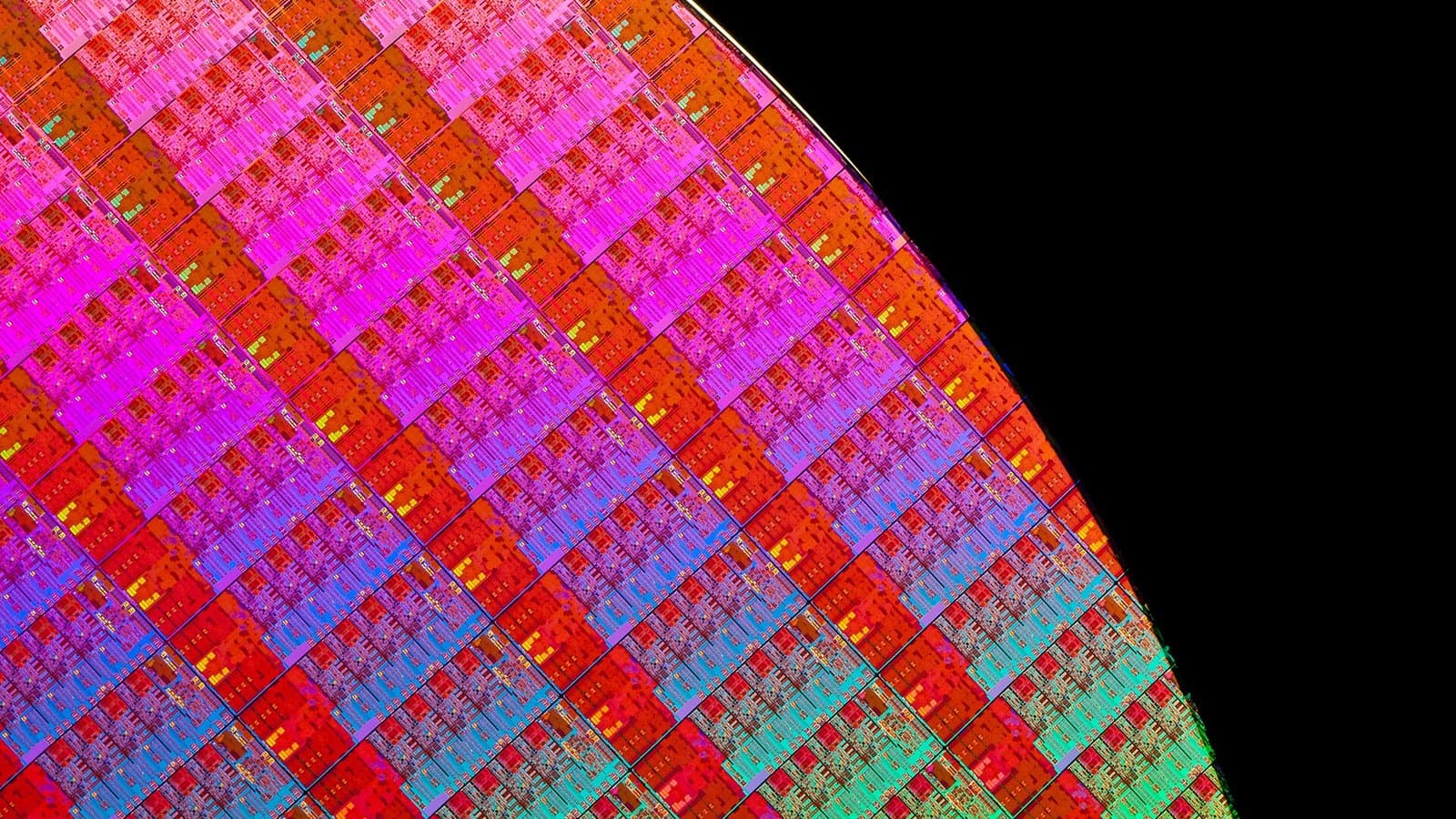
Feature image: a fourth-generation Intel Core processor wafer by Intel in Deutschland, via Wikimedia Commons, CC BY-SA 2.0.
Tags

TPW Editorial
Editorial Team
TechPastWeek's editorial team reports and edits every story we publish. We research each piece against primary and credible secondary sources, and a human editor reviews and signs off before it goes live.