
EUV Lithography, Explained: How the Chip Industry Prints at 13.5 Nanometers
Extreme ultraviolet lithography uses 13.5 nm light from tin plasma to print the smallest chip layers. How EUV works, what it costs, and why ASML controls it.

On this page
Key takeaways
- EUV lithography prints chip features with 13.5 nm light, more than 14 times shorter than the 193 nm wavelength used by DUV immersion systems.
- EUV light is generated by firing a high-power CO2 laser at roughly 50,000 tin droplets per second, creating a plasma that emits at 13.5 nm.
- ASML is the world's only supplier of EUV scanners; a 0.33 NA NXE tool costs about $200 million, and a 0.55 NA High-NA EXE tool costs roughly $350 million or more.
- Current low-NA EUV throughput runs from about 170 to 220 wafers per hour depending on dose, while the High-NA EXE:5200B is specified at 175 wafers per hour at 50 mJ/cm².
- High-NA EUV lifts the numerical aperture from 0.33 to 0.55 and resolution from about 13 nm to about 8 nm, but it exposes only a half-size field and needs a larger reflective mask.
Every advanced logic chip and AI accelerator made today passes through a machine that fires a laser at droplets of molten tin tens of thousands of times a second inside a vacuum, producing light no ordinary material can transmit or bend. That machine is an extreme ultraviolet (EUV) lithography scanner, and it has become the single most concentrated bottleneck in the global semiconductor supply chain.
Related reading: Intel Has Run a Million High-NA Wafers, and Its Rivals Just Adopted Its Standard · Samsung Starts Trial Production of Tesla's AI5 Chip at Its Texas 2nm Fab.
One company, ASML of the Netherlands, builds every EUV scanner in the world. The light these machines use has a wavelength of 13.5 nanometers, which is why they can print circuit patterns far smaller than any earlier technology could. Understanding EUV means understanding two things: why shorter wavelengths set a hard physical limit, and why 13.5 nm light is so awkward that it took more than two decades and billions of euros to turn into a production tool.
What lithography actually does
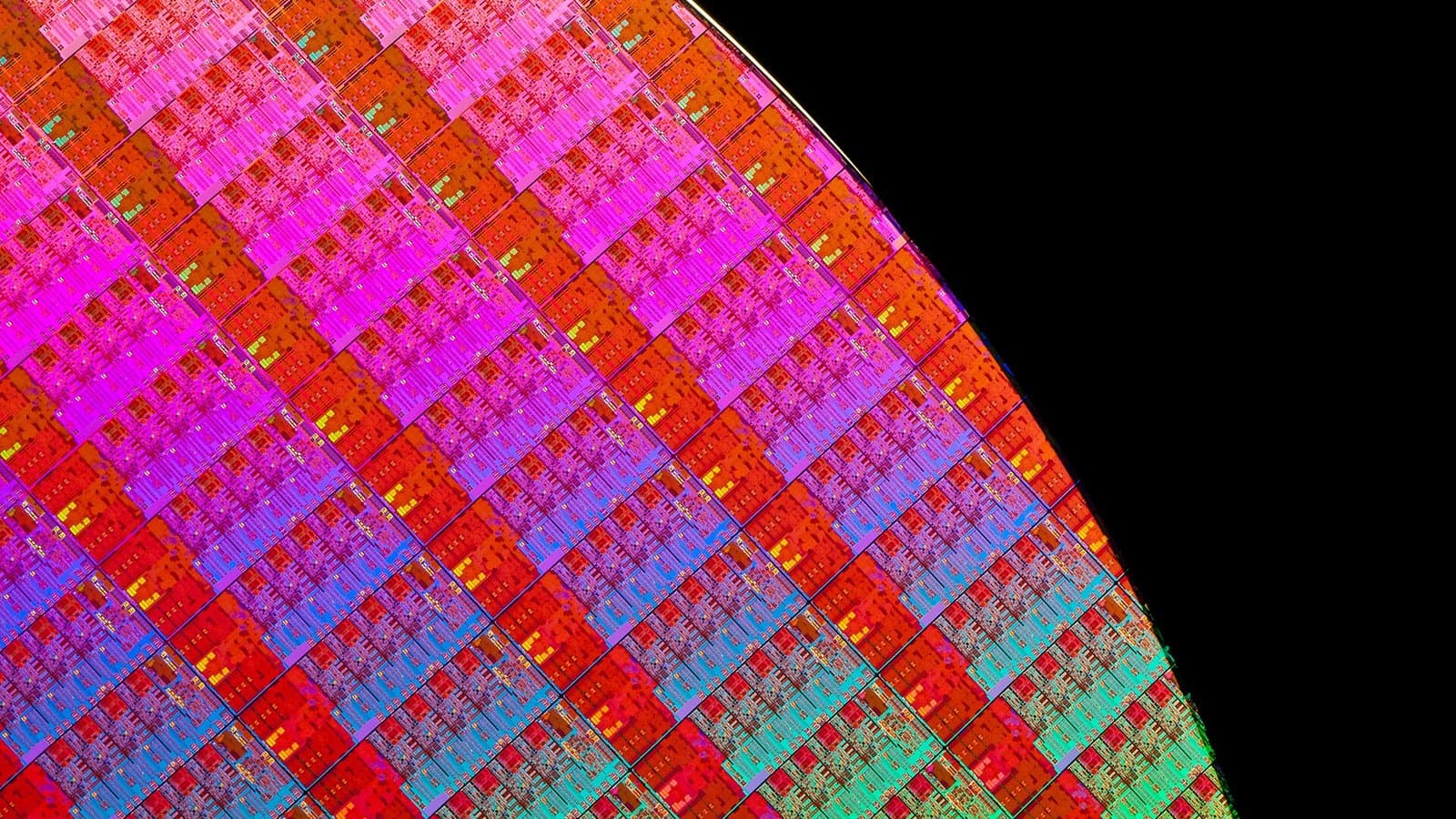
Chipmaking is a printing process repeated dozens of times. A silicon wafer is coated with a light-sensitive material called photoresist, then exposed to a pattern of light projected through a mask, the chip industry's version of a stencil. The exposed or unexposed regions are dissolved away, and the resulting pattern is etched into the wafer or used to build up another layer of transistors and wiring. A leading-edge chip stacks many such layers, so the cost of each one adds up.
The smallest feature a system can print follows the Rayleigh criterion:
    CD  =  k1  x  ( wavelength / NA )

    CD   = critical dimension (smallest printable feature)
    k1   = process-dependent factor, physical floor near 0.25
    NA   = numerical aperture (the cone of light the optics can collect)
Resolution improves when the wavelength shrinks or the numerical aperture grows. For years the industry advanced by pushing both. Argon fluoride (ArF) excimer lasers gave 193 nm light, and immersion lithography boosted the effective aperture by placing water, with a refractive index near 1.44, between the final lens and the wafer. That dropped the effective wavelength to roughly 134 nm and allowed numerical apertures above 1.0.
That path has a floor: no fluid has a high enough refractive index to keep the trick working at much finer scales. So at the tightest pitches, 193 nm immersion was stretched by multi-patterning: splitting one dense pattern into two or more simpler masks and exposures, then combining them. Techniques such as self-aligned double and quadruple patterning (SADP and SAQP) can reach features far smaller than a single exposure allows. They also multiply the number of deposition, etch, and alignment steps, and every added step costs money and can introduce defects. A 193 nm SAQP flow carries roughly three times the normalized wafer cost of a single 193 nm immersion exposure, according to a widely cited patterning cost comparison.
Why the industry moved to 13.5 nm
EUV changes the wavelength itself. At 13.5 nm, the light is more than 14 times shorter than DUV's 193 nm. At a numerical aperture of 0.33, ASML rates its NXE systems for 13 nm resolution, which is out of reach for DUV. Without EUV, the industry would need layer after layer of multi-patterning, each one adding cost and chance of failure.
The resolution equation, in one line
Shorter wavelength and higher numerical aperture mean smaller features. EUV shrinks the wavelength more than fourteenfold. High-NA then raises the aperture from 0.33 to 0.55.
How EUV light is made
Producing 13.5 nm light is the hardest part of the system, because it cannot be bought as a laser. It has to be created as a byproduct of a violent, controlled explosion.
The process, as ASML and its partners describe it, works like this:
- A generator ejects molten tin droplets of about 25 microns in diameter at roughly 70 meters per second.
- A high-power carbon dioxide (CO2) laser from the German company TRUMPF fires two pulses at each droplet. The first, lower-energy pre-pulse flattens the droplet into a pancake. The second, far more powerful pulse vaporizes it.
- The tin becomes a plasma heated to around 200,000°C to 220,000°C, tens of times hotter than the surface of the Sun, which emits extreme ultraviolet light peaking near 13.5 nm.
- A large collector mirror gathers that light and directs it into the optical system.
This cycle repeats 50,000 times per second. The energy conversion is poor: only a small fraction of the laser's power emerges as in-band EUV. That inefficiency is why the light source is a 250-watt-class module that consumes over a megawatt at the wall, and why ASML is working to reach a 1,000-watt source and 330 wafers per hour by 2030. The complete NXE system weighs about 180 metric tons.
  tin droplets --> CO2 laser (2 pulses) --> plasma --> EUV light
                                                          |
                                              collector mirror
                                                          |
                         illuminator mirrors --> reflective mask
                                                          |
                        projection mirrors (6, all reflective)
                                                          |
                                                  wafer in vacuum
Mirrors, vacuum, and the price of opacity
Almost every material absorbs extreme ultraviolet light, including air. There is no glass lens that can transmit it, so EUV systems use mirrors rather than lenses, and the entire light path sits in a high vacuum.
Each mirror is a molybdenum and silicon multilayer, a stack of dozens of alternating layers just a few nanometers thick that reflects EUV through constructive interference. Even a perfect multilayer mirror reflects only about 70 percent of the light that hits it, and the projection optics alone may use six mirrors. With the mask and illuminator, the beam can bounce off roughly ten surfaces before it reaches the wafer, so a large share of the light generated in the plasma never arrives. Zeiss SMT makes these optics.
The plasma is destructive: tin debris and ions bombard the collector mirror, which must be cleaned continuously and is effectively a consumable, replaced on a regular cycle.
The mask and the resist
An EUV mask is not a transparent stencil. It is a reflective plate: a multilayer mirror blank with a patterned absorber layer on top that blocks the light where the circuit pattern should not print. Because the light strikes the mask at an angle and the absorber and multilayer interact in three dimensions, EUV masks behave differently from DUV masks and are expensive to make and repair.
On the wafer, the photoresist receives photons with an energy of 91 to 93 electron volts, roughly fourteen times that of a 193 nm photon. The higher energy starts a chain of secondary electrons, which is useful, but it also sharpens a problem known as stochastic behavior: because relatively few photons arrive in a tiny area, random variations in how many photons and electrons land where can leave a line slightly rough or cause an occasional defect. Resist makers and chipmakers respond by raising the exposure dose, and higher dose means lower throughput. That trade among resolution, defect rate, and speed is a central tension of EUV production.
Where EUV's resolution floor really sits
At very small features, the random arrival of photons and the chemistry of the resist set a practical floor beyond what the optics dictate, which is why even EUV needs multi-patterning at the tightest pitches.
Throughput, cost, and the multi-patterning question
Throughput is measured in 300 mm wafers per hour, and it depends heavily on exposure dose. ASML specifies the earlier NXE:3400C at 170 wafers per hour at a 20 mJ/cm² dose, dropping to 135 at 30 mJ/cm². The NXE:3600D improved that by 15 to 20 percent. The NXE:3800E, aimed at 2 nm logic and leading-edge DRAM, is quoted at 220 wafers per hour at 30 mJ/cm².
Throughput, not purchase price, dominates cost per wafer: a scanner costing hundreds of millions must expose a great many wafers to justify itself. ASML's 0.33 NA NXE tools run about $200 million each, and High-NA EXE tools are reported at $350 million or more. EUV also draws far more power than DUV: roughly 1.31 megawatts versus 0.13 megawatts in a comparison of an NXE and an immersion tool, and its throughput per pass is lower.
The economics of replacing multi-patterning are genuinely contested. ASML's own modeling presented at industry conferences claims roughly a 35 percent cost benefit for High-NA single-exposure logic metal and about 20 percent for random vias compared with multi-patterning. Analysts at SemiAnalysis have argued the opposite for some cases, concluding that High-NA single patterning can cost significantly more than double-patterning on existing low-NA machines. TSMC's Kevin Zhang, whose company runs some of the most EUV hours on earth, has called High-NA “very, very expensive”.
The practical result is that EUV did not make DUV obsolete. It is reserved for the densest, most critical layers. ASML still ships around 130 DUV immersion systems a year against roughly 65 low-NA EUV systems, and most layers on a modern chip are still printed with DUV.
Why EUV is the chokepoint
A chip design can be ready and the logic wafers can be available, but the product cannot ship without a scanner to print the critical layers. Because one company makes all of them, ASML's production rate sets the ceiling on how fast the industry can add leading-edge capacity.
The ASML monopoly and its supply chain
ASML is the only company that makes EUV scanners, and its 2024 annual report states the position plainly: the company is the world's only manufacturer of EUV lithography systems. Its dominance rests on partners that are themselves irreplaceable. Zeiss SMT supplies the EUV optics, TRUMPF supplies the high-power CO2 drive laser, and Cymer, which ASML acquired in 2013, builds the light source. The supply chain is deep and narrow at the same time.
That matters for capacity math. ASML produced around 65 low-NA EUV systems in 2026 and planned to add 30 percent more capacity in 2027, with a further 30 percent under study for 2028. Every leading-edge fab expansion depends on getting those tools. The chokepoint is also political: EUV scanners are subject to Dutch and aligned export controls, and ASML does not ship them to China.
High-NA: the same light, a bigger cone
High-NA EUV does not change the wavelength. It changes the optics. The EXE platform raises the numerical aperture from 0.33 to 0.55, a 67 percent increase, and ASML rates it for 8 nm resolution with 40 percent more imaging contrast. At the same 13.5 nm wavelength, that pushes the theoretical printable half-pitch from about 13 nm to about 8 nm.
Getting there forced major engineering changes. The optics are anamorphic, meaning they reduce the pattern by different factors in the two directions, and they use eight projection mirrors instead of six. The exposure field is halved to 26 by 16.5 millimeters, so a full chip is stitched from multiple exposures, and the mask grows to a new 6 by 10.5 inch format. The EXE:5200B production tool is specified at 175 wafers per hour at a 50 mJ/cm² dose with 0.7 nm overlay.
The first High-NA system shipped in December 2023, and Intel took the first production EXE:5200B and is using it for selected layers of its 14A node. TSMC has been more cautious and may steer around High-NA for its next node. High-NA is a beachhead, not yet a fleet, and it does not replace standard EUV, which remains the volume workhorse.
High-NA does not mean 8 nm chips
A process node name such as 2 nm is a marketing label, not a measurement. High-NA's 8 nm figure is the resolution of the imaging system, not the transistor size on the final chip.
The trade-offs, stated plainly
EUV is a bundle of difficult compromises. Shorter wavelength buys resolution but forces a vacuum, reflective optics, and a light source that wastes most of its energy. The higher photon energy enables fine chemistry but introduces stochastic defects that push dose up and throughput down. The machines deliver smaller features in fewer steps but cost hundreds of millions of dollars each and run at lower throughput than the immersion tools they partly replace.
The result: “smaller wavelength” is not automatically “cheaper.” Choosing among EUV, DUV multi-patterning, and High-NA on any given layer is a cost-per-layer calculation that varies by pattern, by fab, and by the EUV hours a company already owns. That is why all three technologies coexist.
What to watch
- Source power and throughput. ASML's target of a 1,000-watt source and 330 wafers per hour by 2030 is the clearest lever on EUV cost per wafer.
- High-NA adoption. Intel's 14A ramp is the first real test. Whether TSMC and Samsung follow will decide how quickly High-NA becomes a fleet rather than a beachhead.
- Hyper-NA. A 0.75 numerical aperture generation sits on ASML's longer-term roadmap, but it is not committed and would demand even more extreme optics.
- Capacity and export controls. Tool availability and Dutch export licensing will shape which countries can produce leading-edge chips at all.
- Alternatives. Canon's nanoimprint tools and Substrate's accelerator-based X-ray lithography approach the same problem differently, though none is a near-term replacement.
The bottom line
EUV lithography turned a physics problem, how to print with 13.5 nm light, into the defining industrial chokepoint of modern computing. The wavelength sets what chips can do; the machine that harnesses it, and the single company building it, set what the industry can make and how fast.
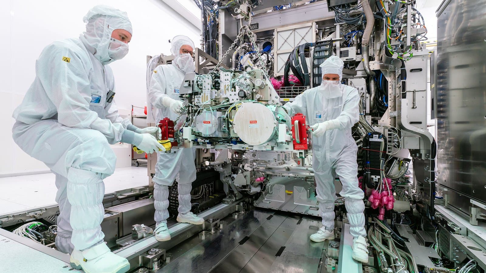
Cover image ©ASML.
Tags
Frequently asked questions
- What wavelength does EUV lithography use?
- EUV lithography uses extreme ultraviolet light with a wavelength of 13.5 nanometers. That is more than 14 times shorter than the 193 nm light used by deep ultraviolet immersion lithography, which is what lets EUV print smaller features in a single exposure.
- Why does EUV use mirrors instead of lenses?
- Almost every material absorbs extreme ultraviolet light, including air. There is no practical transparent lens material at 13.5 nm, so EUV systems shape the beam with multilayer reflective mirrors inside a high-vacuum chamber instead of glass lenses.
- How much does an EUV lithography machine cost?
- A standard 0.33 numerical aperture NXE system costs roughly $200 million, while a 0.55 numerical aperture High-NA EXE system is reported at around $350 million to $400 million. The machine is the single most expensive tool in a leading-edge fab.
- Does High-NA EUV replace multi-patterning?
- Only on selected critical layers. High-NA EUV can print some patterns in one exposure that older 0.33 NA EUV needs multiple passes to produce, but most chip layers are still printed with DUV immersion and multi-patterning, and even EUV needs multi-patterning below roughly a 30 nm pitch.

TPW Editorial
Editorial Team
TechPastWeek's editorial team reports and edits every story we publish. We research each piece against primary and credible secondary sources, and a human editor reviews and signs off before it goes live.