TSMC's A16 Is Ready: Backside Power Meets the Angstrom Era
TSMC has completed development of its 1.6nm-class A16 process with Super Power Rail, targeting Q4 mass production for AI and HPC customers.

On this page
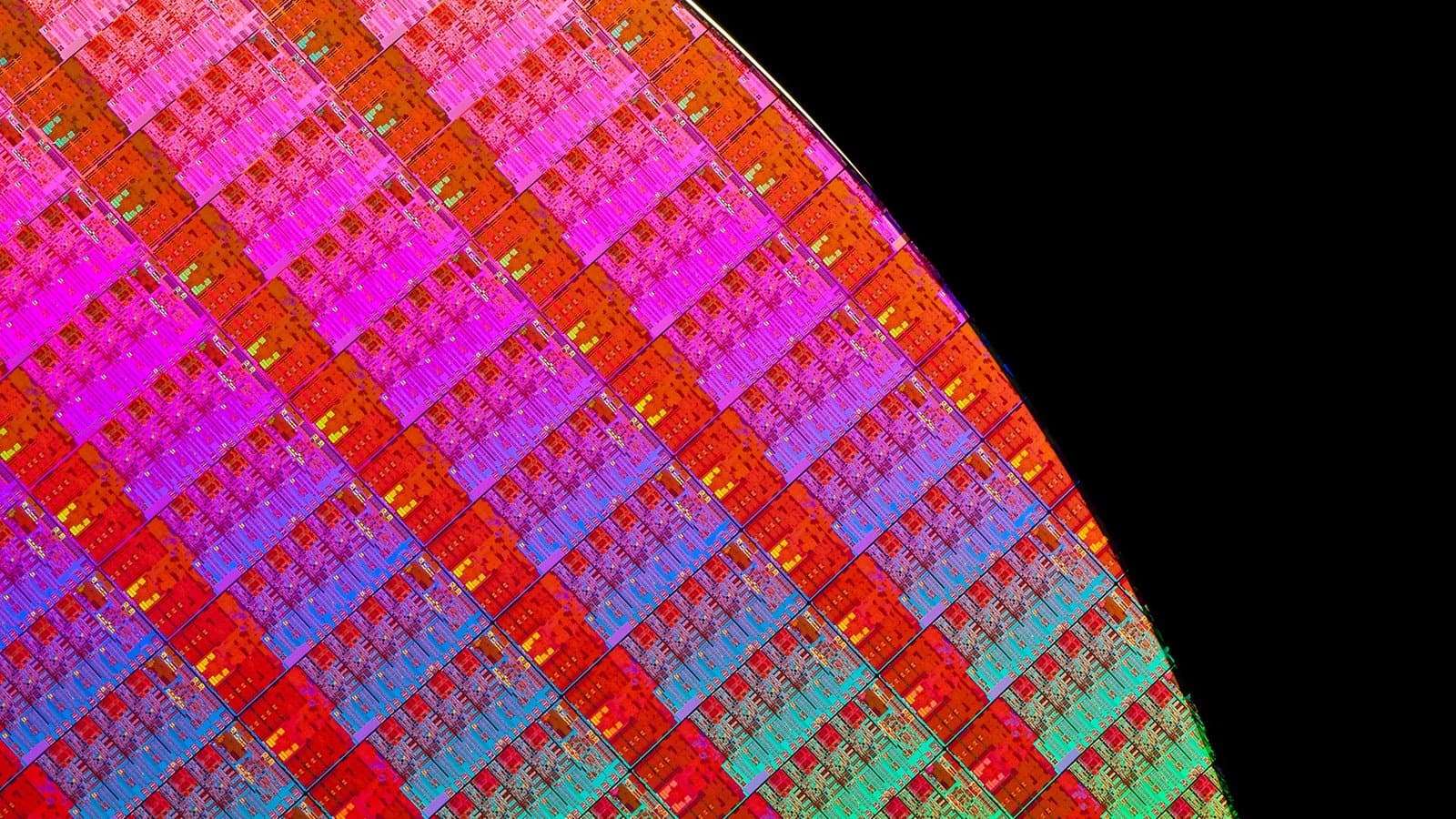
TSMC has completed development and validation of A16, its 1.6-nanometre-class process, and is preparing to begin mass production in the fourth quarter of 2026. The milestone, reported by Taiwan and Korean trade outlets in the third week of August and confirmed by TSMC's own technology documentation, makes A16 the first "angstrom-class" CMOS platform to ship with backside power delivery, a structural change to how a chip is wired that promises better speed and efficiency at a point when AI accelerators are straining against both.
Related reading: Eight Tech Companies Are Evaluating Intel's 14A Node, and None Has Signed · TSMC's August Revenue Hits a Record NT$514.8 Billion as AI Demand Outruns Supply.
The process pairs TSMC's next-generation nanosheet transistors with a technology the company calls Super Power Rail (SPR). The details matter less than the direction: after decades of building every wire on the front of the wafer, the industry is moving the power network to the back.
What backside power actually does
In a conventional chip, both the signal wiring and the power delivery network sit on the front side of the die, stacked in the same set of metal layers. As transistors shrink, the two networks increasingly compete for the same limited routing space. That competition causes congestion and resistance, and resistance causes voltage drop (the industry's familiar "IR drop"), which wastes power and limits how fast a design can run.
Super Power Rail separates the two. Power is delivered from the backside of the wafer through dedicated vertical backside contacts, or VBs, that run directly to the source and drain regions of the transistor. That frees the front side for signal routing alone. According to Electronic Times, TSMC achieved this while making minimal changes to the front-side gate structure, cell dimensions and layout footprint, a deliberate choice to avoid breaking existing design tools and cell libraries.
The payoff is competitive rather than dramatic. Compared with N2P, TSMC's enhanced 2nm process, A16 is quoted at 8 to 10 percent higher speed at the same power, or 15 to 20 percent lower power at the same speed, with chip density improving by 8 to 10 percent. Those are the kind of incremental, node-on-node gains the industry has trained itself to expect. The significance is that they arrive while preserving design compatibility, which is what determines whether customers can actually adopt a node on a schedule.
The short version
A16 is not a leap in raw performance. It is a leap in wiring. Moving power to the back of the wafer removes a bottleneck that has been getting worse at every node, and it does so without forcing chip designers to redraw their layouts from scratch.
Why "angstrom" is a marketing word and also a real threshold
The semiconductor industry spent the 2010s arguing about what a "nanometre" meant, because the number stopped corresponding to any physical dimension. The shift to "angstrom-class" naming (16 angstroms is 1.6 nanometres) is partly a branding exercise. It signals that a new era has begun, and it gives the foundries a fresh set of numbers to market.
But A16 is also a genuine technical threshold, because it is the point at which backside power delivery arrives in a high-volume commercial process. Intel got there first with PowerVia on its 18A node, and the contrast between the two approaches is instructive. Electronic Times noted that Intel had to modify its existing cell architecture during testing, adjusting pin counts and relaxing metal pitches. TSMC's pitch for A16 is that it does not require that kind of disruption. If that holds in production (always the operative caveat) it lowers the cost of adoption for customers whose designs are already tuned to TSMC's platform.
Development is not volume
Completing development and validation is a real milestone, but it is not the same as shipping millions of good dies. The difficult part of any node is the yield ramp: getting defect densities low enough that a large, expensive accelerator can be built at a price customers will pay. TSMC's Q4 target is a production schedule, not a guarantee of healthy margins on day one.
Who needs it, and why now
The timing is not accidental. A16 is explicitly aimed at AI and high-performance computing, the segments where complex signal routing and dense power networks are hardest to manage and where customers will pay a premium for efficiency. Data-centre accelerators are now among the largest and most power-hungry chips ever built, and their economics are increasingly dominated by how much useful computation they deliver per watt.
For the hyperscalers and chip designers who buy leading-edge capacity, backside power is attractive for a second reason: it can make an existing design faster without requiring a new microarchitecture. When a product cycle is measured in months and a design respin costs a nine-figure sum, a process that improves power and speed while preserving the design is worth a great deal. That is the commercial argument for A16, and it is stronger than the raw performance numbers suggest.
TSMC is not standing still after A16. The company has said the next step is A14, a 1.4nm-class process targeted for mass production in 2028, and it continues to spend heavily: on August 11, its board approved capital expenditure of $29.44 billion for advanced process and packaging capacity. The A16 milestone matters partly as evidence that the company's roadmap is intact at a moment when the cost of each new node is rising faster than the number of customers who can afford to use it.
The economics of a leading-edge node
A16's technical case is straightforward; its business case is harder. Leading-edge nodes have become progressively more expensive to develop, and the capital required to build capacity for them has risen even faster. TSMC's $29.44 billion capital-expenditure approval in August is one data point; the broader trend is that only a handful of companies can afford to design chips on the newest process, and only a few end markets (AI accelerators chief among them) can absorb the cost of doing so.
That concentration creates a self-reinforcing dynamic. The customers who can pay for the newest node get the best efficiency, which lowers their operating costs at scale, which lets them buy more of the newest node. A16 will be judged not only by how fast its transistors switch, but by whether the company can deliver complete packaged solutions in the volumes its customers need.
Packaging is the other half of this equation. An advanced logic die is only useful once it is combined with memory and other chiplets in a package, and advanced packaging capacity has been one of the tightest links in the AI supply chain. TSMC's decision to spend on process and packaging capacity in the same capital plan reflects that reality. The node is necessary but not sufficient; the scarce resource is finished, tested, packaged silicon.
The competitive frame
TSMC's lead in leading-edge logic is not new, but the basis of that lead is shifting. For years the company's advantage was execution. It hit its nodes on time while rivals stumbled. Now the differentiator is increasingly the design ecosystem: the libraries, tools and packaging options that let customers turn a process into a product. Backside power raises the stakes on that front, because a node that requires designers to change their standard cells is a node that gets adopted more slowly, no matter how good its transistors are.
Intel's PowerVia was an early demonstration that backside power works, and Samsung is pursuing its own version. The race is not really about who announces first; it is about who reaches volume production with acceptable yields and a design ecosystem customers can use. On that measure, A16's completion is less a victory lap than the start of the hard part.
There is also a demand-side question that no process announcement can answer. The leading-edge foundry market is a small oligopoly serving a handful of very large customers. If AI infrastructure spending cools, or if the largest buyers shift more of their workload to cheaper, older nodes, then part of A16's projected value evaporates. The node is being readied for a boom; whether the boom arrives on schedule is a separate bet.
What to watch in the Q4 ramp
The number that will matter is not the speed gain in TSMC's marketing slides. It is how quickly A16 reaches the utilisation levels that let TSMC price it profitably, and whether the first customer designs tape out without the kind of layout rework that would erode the compatibility promise.
What it means beyond the fab
The A16 story is also a reminder of how concentrated the most advanced chipmaking has become. A single company in Taiwan, using tools from a small number of suppliers and a power architecture pioneered in part by Intel, sits at the base of the entire AI economy. That concentration is why governments from Washington to Brussels have spent billions trying to build alternatives, and why every node transition is watched as closely for its geopolitical signal as for its technical specs.
The technical signal from A16 is clear: backside power is no longer an experimental curiosity but a mainstream tool of the next node. The geopolitical signal is more ambiguous. TSMC's ability to deliver it on schedule reinforces its centrality rather than dispersing it, at least for now.
What to watch
Three things will show whether A16 meets expectations. First, the yield ramp in the fourth quarter and early 2027, which determines whether the node is a commercial success or merely a technical one. Second, customer adoption, particularly whether a flagship AI accelerator on A16 appears on the timetable its buyer has signalled, or slips. Third, the competitive response, as Intel and Samsung push their own backside-power nodes toward volume and the marketing contest over process leadership intensifies.
The bottom line
A16 is a milestone that deserves the word. It closes the development phase on the first high-volume process to move power delivery to the back of the wafer, and it does so with a design-compatibility story that could matter more than the advertised speed gains. The next chapter is not about whether the technology works (that is now established) but about whether the industry can manufacture it at the scale and cost that AI's appetite demands. That is a harder problem, and it will not be solved by an announcement.
Tags

TPW Editorial
Editorial Team
TechPastWeek's editorial team reports and edits every story we publish. We research each piece against primary and credible secondary sources, and a human editor reviews and signs off before it goes live.